3nm in Samsung Plans for 2021
Article By : Dylan McGrath, EE Times
Outlines future roadmap, starting with 7nm EUV during second half of 2017
SANTA CLARA, Calif. — Samsung Electronics laid out plans to bring to mass production in 2021 the architectural successor to FinFETS, gate-all-around (GAA) transistors, at the 3nm node. The South Korean giant also reaffirmed plans to begin 7nm production using extreme ultraviolet (EUV) lithography in the second half of this year at its annual foundry technology forum here Tuesday (May 22).
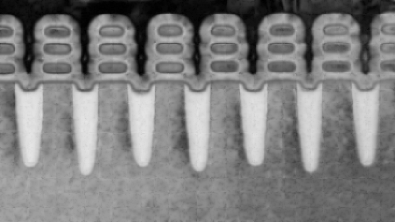
GAA technology has been under development since the early 2000s by Samsung and other firms. GAA transistors are field-effect transistors (FET) that feature a gate on all four sides of the channel to overcome the physical scaling and performance limitations of FinFETs, including supply voltage.
Samsung’s proprietary GAA technology, known as multi-bridge-channel FET (MBCFET), has been in development since 2002, according to Ryan Sanghyun Lee, vice president of market for Samsung Foundry. MCBFET uses a nano-sheet device to enhance gate control, significantly improving the performance of the transistor, according to the company.
Samsung said last year that it planned to use GAA transistors at the 4nm node starting in 2020. However, industry watchers expected GAA to be in production no earlier than 2022.
Samuel Wang, a vice president in foundry research at Gartner, said he had expected Samsung to have GAA transistors production ready some time in 2022. “It looks like they are moving faster than that,” Wang said.

“The Samsung roadmap was aggressive,” said Kevin Krewell, I already knew they were moving fast on EUV, but this also sets a high bar.”
But, Krewell added, “It’s still a ways out and schedules can slip.”
Last June, IBM and its research alliance partners Samsung and Globalfoundries described the process they had developed for making 5nm GAA transistors based on stacked nanosheets at the 2017 Symposia on VLSI Technology and Circuits conference in Kyoto, Japan. Other chipmakers, including Intel and TSMC, are known to be developing their own versions of next-generation transistors beyond FinFET similar to GAA FETs.
Samsung reiterated plans to begin using EUV lithography in mass production in the second half of this year with its 7nm Low Power Plus process. Samsung is expected to be the first chipmaker to put EUV — which the industry has been developing for many years — into commercial production. TSMC and Globalfoundries have announced plans to use EUV in commercial production starting in 2019.
While lithography tool vendor ASML and leading-edge chip makers have demonstrated the ability to overcome the source-power issue that plagued EUV development for years, the supporting technologies needed to deploy EUV in commercial production are still being developed and fine-tuned.
Yongjoo Jeon, a principal engineer with Samsung Foundry, said Tuesday that Samsung will use an internally developed EUV mask inspection tool. This is a significant advantage for Samsung, since no commercial tool has been developed, Jeon added.
Jeon said that Samsung will initially deploy EUV without the benefit of a pellicle to protect EUV photomasks from particle contamination, another technology that is still in development. Jeon said Samsung is making progress on developing an EUV pellicle and that he is confident that the company will eventually have one to deploy in its EUV process.
Samsung is also still developing EUV photoresist and is on track to be able to achieve the target defect density for mass production later this year, Jeon said.
Samsung’s process technology roadmap also includes 5nm FinFET production in 2019 and 4nm FinFET production in 2020.
— Dylan McGrath is the editor-in-chief of EE Times.

Subscribe to Newsletter

Test Qr code text s ss
