S/TEM combines hi-res, high-throughput analytics
Article By : Thermo Fisher
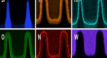
The Themis S S/TEM includes optics, chemical detection, wide gap pole-piece and unique application software that ensures the platform covers a wide range of applications.
Thermo Fisher Scientific Inc. has launched the Themis S S/TEM, an 80–200kV scanning/transmission electron microscope (S/TEM) designed for high-speed imaging and analysis of semiconductor devices.
Included in the industry-standard Themis TEM platform, the Themis S TEM offers a combination of spatial resolution and chemical analysis. The system claims to resolve the needs of semiconductor failure analysis labs working at the sub-20nm technology node. It includes an integrated vibration isolation enclosure and full remote operation capability. Its additional features such as probe-corrected, 80–200kV column, automated alignments, XFEG source and DualX X-ray spectrometre provide robust, sub-Ångström imaging and fast, accurate elemental and strain analysis, Thermo Fisher said.
Themis S S/TEM achieves fast time to data by using a combination of the Piezo stage and drift corrected frame integration (DCFI) to compensate for possible specimen drift. This makes it possible to acquire high-quality, high-resolution images in both TEM and STEM modes only minutes after sample loading, Thermo Fisher noted.
To optimise productivity, Themis S S/TEM uses double-coil constant power lenses to minimise the thermal drift and maximise the system throughput. This design eliminates heating variation in the lens when switching between modes, such as changing from low-magnification mode for feature searching and high-magnification mode for imaging, the company said.

Subscribe to Newsletter

Test Qr code text s ss
