PCB tech shrinks designs with 25µm linewidth
Article By : Graham Prophet
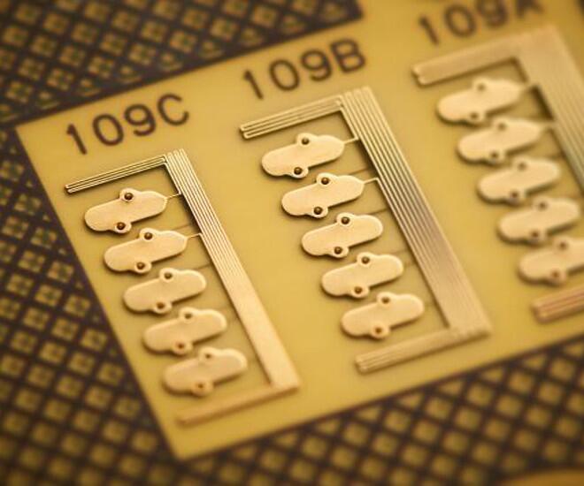
DenciTec enables the production of circuits with extremely high density without the disadvantages of the established manufacturing processes.
Switzerland-based Cicor has rolled out a technology platform called DenciTec that offers very small 3D PCBs aimed at high density designs, especially medical applications, such as neurostimulators, catheters, insulin pumps, cochlear implants, intelligent prosthesis control, lab-on-a-chip, ultrasonic measuring heads and micropumps.
The company says that the boundaries between thin-film and printed circuit technology is becoming increasingly blurred. With classic semi-additive processes using thin-film technology, conductor widths and spacings of less than 15µm can be achieved. However, this technology is usually limited to production formats that result in less attractive product prices. It is technically possible for this technology to be upscaled, but this is complicated and expensive.
The DenciTec platform enables the production of circuits with extremely high density without the disadvantages of today's established manufacturing processes. The possibilities include conductor widths and spacings down to 25µm with copper thicknesses of 20µm ±5µm on all conductive layers, laser-via diameters of 35µm, annular rings with a diameter of 30µm for the inner layers and 20µm for the outer layers, copper-filled blind vias with the option of via stacking, and vias-in-pads. The use of advanced materials allows the production of ultra-thin circuits, including, for example, the manufacture of 4-layer flex circuits with a total thickness of less than 120µm.

Subscribe to Newsletter

Test Qr code text s ss
