Make the best ADC-MCU connection
Article By : Bonnie Baker, John Zhonghua Wu

A wide array of precision devices is readily available to designers building high-performance systems. For those systems, layout and design are very important. And for such systems with multiple boards, board interconnections are a critical piece of the PCB design. While we may pay little attention to interconnection details on the assumption they don’t apply […]
Connecting a relatively “slow” ADC with a 2.25MHz clock across a short, 1m wire to the MCU is as easy as buying and plugging in the wires. However, a poor PCB interconnection design can easily damage a good design using fabulous parts.
 |
|
Figure 1: Physical arrangement of the ADS8326 EVM and the MSP430F449 board connected by a 1m twisted-pair cable is shown. |
This article focuses on the critical factorsand what could be seen as “surprises”whenever pursuing a high-performance PCB interconnection system.
Figure 1 shows a 1m CAT-5 twisted-pair cable connecting a successive approximation register (SAR) ADC, represented by the ADS8326, and an MCU, represented by the MSP430 evaluation board (EVM). The ADS8326 is a 16bit, high-speed, 2.7-5.5V micropower ADC. The system clock frequency for this device ranges from 24kHz to 4.8MHz.
The MCU transmits a 2.25MHz clock and chip select signal across the CAT-5 cables to the ADC as shown in Figure 2. The ADC responds by transmitting the conversion data back to the MCU.
Because of the slow clock rate, termination issues between these two devices were not apparent at first. Surprisingly, we found that transmission data between the boards, combined with the mismatched characteristic impedances, caused significant reflection errors across the 1m loop. These reflections distorted the clock and data signals between the boards.
Figure 3 shows what happens when line impedances between two boards are overlooked. CH1 shows the 2.25MHz clock signal transmitted from the MCU side of the circuit to the ADC board. The ADC uses this clock signal to synchronize data transmitted back to the MCU. CH4 shows the data’s arrival from the ADC at the MCU.
Both channels show that signal distortion exceeds high-level and low-level thresholds, with significant signal overshoot and undershoot occurring. These signals have false edges, or ringing and reduced operating margins. Looking at the ADC side of the circuit, we can see similar effects.
Our immediate response to the ringing reflected in Figure 3 is to slowdown the clock’s frequency. You may find a quick and successful fix, or you may be challenged. Engineers are often convinced that the clock rate dictates the type of PCB to be implemented, thus ignoring the clock’s rise and fall times or switching times. However, to tame transmission-line effects, define your highest-frequency signal based on switching times, not signal frequencies.
Transmission operation
High-performance interconnect systems require attention to long-transmission line issues, such as reflection and termination. The actual clock frequency describes the clock or data rate in the application. In our test circuit, this frequency is 2.25MHz. The effective operating frequency (EOF) of a PCB is defined as:
 |
where the signal’s EOF is equal to the system’s EOF, tRISE is equal to the rise time and tFALL is equal to the signal’s fall time. Equation 1 defines the signal’s rise and fall times:
 |
For a worst-case calculation, use the smaller value between tRISE and tFALL.
When determining the rise time on the bench, be aware of any test equipment limitations. Using an oscilloscope display, calculate the switching signal‘s rise and fall times, and EOF by inspection. For instance, if the measured signal’s rise time is 2ns, the signal’s EOF is 175MHz.
Equipment errors can be accounted for with a formula that uses the square root of the sum of the squares, or root sum square (RSS). For instance, the bandwidth of your probe can be 500MHz, while the oscilloscope’s bandwidth is 350MHz. Using an RSS formula, the measured rise time of a 2ns signal, with the equipment limitations above, is actually equal to 1.6ns. Now calculate this using the following formulas:
 |
Using this calculation, the switching signal is 221MHz.
This is far above the ADC’s actual operating clock frequency (2.25MHz) and the previously calculated EOF of 175MHz.
Signal’s rise and fall
Now that we have determined the system’s EOF, let’s characterize the connections between the MCU and the ADC by defining the critical length of our transmission line. In our test system, signal rise time, propagation delay and cable length are related.
 |
|
Figure 2: A CAT-5 twisted-pair cable carries the clock and chip select signals from the MCU to the data converter. (Click to view full image) |
Propagation delay is the time required for a signal to travel from a driver to a receiver. A major high-speed PCB design challenge is to make sure this delay time is less than the signal’s rise or fall time.
If the signal propagation delay time (TPD) is less than one-seventh of tRISE (RISE), we can model the connection as an inductive-capacitive pi model (LC pi model). If tRISE is greater than the propagation delay time, we’ll use the microwave theory to model the board interconnection transmission line.
In contrast, if the lines are sufficiently short, the signal will rise during the line’s propagation delay, and the reflection becomes part of the rising edge. With longer connection lines, the propagation delay may be greater than the signal’s rise time, and reflections appear as an overshoot or undershoot.
TPD is proportional to the relative dielectric constant of the twisted-pair wires (Equation 2):
 |
For AWG 24-wire, the typical TPD is approximately equal to 52.7ps/cm. As long as a cable length is longer than 4.27cm and the signal switching time is less than 1.6ns, the transmission-line model is required to analyze the cable.
In transmission-line theory, the voltage and current along a transmission line can vary in magnitude and phase as a function of position. ZO is the characteristic impedance of the transmission line when it is infinitely long or ideally terminated.
The twisted pair cable formula for its characteristic impedance is Equation 3:
 |
where Er is the relative dielectric constant of the cables.
The wire’s insulator and air permittivity determine the value of Er. The distance between the cables is D, and the diameter of the cable wires is a.
For an AWG 24-wire where D is equal to 0.038 inch, a will be equal to 0.02 inch, Er to 2.5 and ZO to 101.
The transmission line’s characteristic impedance largely influences the transient response of a signal passing through it.
The voltage reflection coefficient (‘) is the amplitude’s ratio of the reflected voltage wave to the incident voltage wave.
ZL is the load impedance (Equation 4):
 |
If the load is mismatched to the line, the incident wave will be reflected at the line and load’s interface. Consequently, power delivered to the load will be reduced. This is also called return loss (RL).
 |
| Figure 3: The MCU generates the conversion clock signal (CH1) and sends it to the ADC. CH4 shows the MCU receiving conversion data from the ADC. |
For our test system, the driver (MCU) has an internal source resistance of 20. The cable characteristic impedance (ZO-430) is close to 100, and the receiver’s input impedance (ADC) is 1G. The output impedance of the driver (ZO-8326) may change with current demand or vary from device to device. The receiver’s input impedance (ZL-8326) may be greater than 1G. An infinite value for ZL produces a reflection coefficient of 1.
A digital rising edge acts like a pure AC signal. When an AC signal reaches the end of the transmission-line path with a mismatch between ZO and the termination ZL, a portion of the wave (up to 100 percent when reflection = 1) is reflected.
 |
| Figure 4: Shown is a signal being reflected between a MCU driver pin and the ADC receiver pin. |
When the wave reflects back along the transmission line, it eventually reaches the original source. If a mismatch exists between ZO and the source impedance (ZS), some portions of the wave are again reflected. The superposition of these reflected waves can cause significant signal degradation.
 |
|
Figure 5: A timing diagram of the signal’s theoretical reflections and the actual ringing at the ADC receiver and MCU driver are shown. (Click to view full image) |
With Figure 4, the reflection factor at the receiver end is 1, and the reflection factor at the driver end is -0.8. From those two numbers, we can calculate the exact ringing amplitude at any time during the signal’s propagation. The initial driver signal is 3.3V.
When a signal transmission is initiated (Figure 4), a 3.3V signal on the MCU’s drive side transmits to the ADC. When this signal is initiated, voltage at the MCU is equal to 2.75V because -0.8 is the reflection factor at the MCU interface. After one propagation delay period or TPD, a 5.5V signal appears at the ADC interface. At this receiver side, the refection factor is 1.
After two propagation delay periods, the signal appears back at the MCU interface. When the signal appears at the MCU, its magnitude is equal to 3.2V. After three propagation delay periods, a 0.9V signal appears at the ADC interface.
Figure 5 illustrates the signal’s reflection and ringing at the MCU driver and ADC receiver.
Circuit termination
Termination is required when the two-way total propagation delay is greater than or equal to the signal rise time, or 2 * TPD tRISE. If source impedance is not matched, the signal at the load will be distorted.
Therefore, be sure to terminate the cables when cable propagation delay exceeds half of tRISE. A good termination happens when the characteristic impedance matches the source and load impedance.
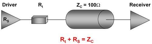 |
| Figure 6: In a source series-termination scheme the driver resistor matches the cable’s impedance (ZC) vs. matching impedance at load (ZL). |
In a source series-termination scheme (Figure 6), the driver resistor matches the cable’s impedance (ZC) vs. matching impedance at load (ZL). Since the driver output impedance is lower than 100, add a series resistor to the signal source impedance to match the cable impedance.
From a practical standpoint, termination only at one end of the transmission line often is adequate and is commonly used.
If we use the same circuit in Figure 1 and pay attention to termination issues, we can correct most of the clock and data distortion issues at the ADC.
 |
|
Figure 7: By investigating termination issues, this circuit addresses an AC termination comprising a resistor and capacitor in series at the transmission channel receiver side. (Click to view full image) |
Figure 7 shows the proposed termination solution for our test application example. The oscilloscope capture in Figure 8 shows the MCU clock in CH1 and the data return from the ADC in CH4.
The technique in Figure 7 uses an AC termination or a 100 resistor in series with a 220pF capacitor to ground. An AC termination has the lowest power drain because current only flows through the termination resistor when the capacitor is charging.
The time constant of the AC-termination RC pair is equal to three (or more) times the signal’s rise time. As tRISE equals 1.6ns, 13.75x tRISE equals approximately 22ns.
A series termination of 80 is installed at the transmission-line driver side, and AC termination is installed at the receiver side.
Thinking ahead Even though clock speeds in our test application are lower than 30MHz to 40MHz, this high-performance system required attention to long-transmission line issues such as reflection and termination. We delved into the issues behind a twisted-pair cable and found that the slower clock speed of 2.25MHz revealed transmission errors with a simple board-to-board connection.
Additionally, critical factors for achieving a high-performance PCB interconnection system were considered. Moving through the termination discussion, we learned that the highest-frequency signal was determined by the signal’s switching times. We addressed these issues using a twisted-pair cable.
 |
| Figure 8: MCU oscilloscope shows improved signal integrity over Figure 3. |
By analyzing the transmission-line model, we found that a TPD greater than 15 percent of the signal’s rise time dictated which termination technique to use.
– Bonnie Baker, John Zhonghua Wu
Senior Application Engineer
Texas Instruments Inc.

Subscribe to Newsletter

Test Qr code text s ss
