Key Highlights From MEMS & Imaging Sensors Summit
Article By : Nitin Dahad, Anne-Françoise Pele
Sub-retinal chips! Tracking down intransigent parking malefactors! Tiny insta-labs! The fun has started.
GRENOBLE — The last half century has seen one technological wave after another, each with its own focus, from the personal computer and microprocessor to wired telephony and then on to mobile phones and smartphones. The next wave will be about connecting the physical world with the digital world, with a focus on sensors.
The annual MEMS & Imaging Sensors Summit in Grenoble, organized by SEMI, is a premiere place to discover what the established large players and emerging startups are developing to bring us ubiquitous sensing. EE Times correspondents have been regular attendees at the conference, and we were back this year for a packed two-track conference covering MEMS and imaging sensors.
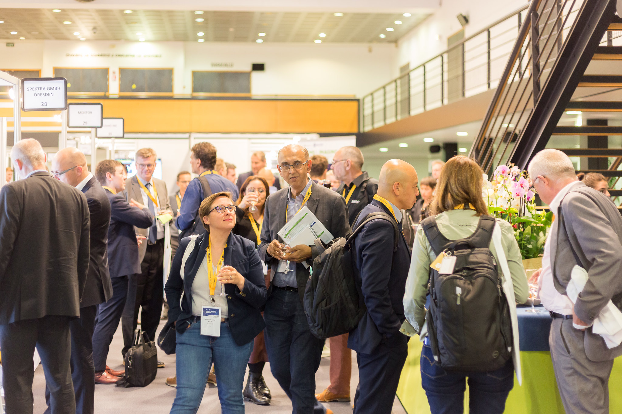
Our EE Times correspondents Anne-Francoise Pele and Nitin Dahad on the beat at the MEMS & Imaging Sensors Summit in Grenoble, France
(Image: SEMI)
The sessions covered everything from business and market forecasts to technologies, manufacturing, applications and of course, a technology showcase from a number of startups which often emerge as spinouts from the bedrock of research institutes such as Leti in France, imec in Belgium, ETH in Switzerland and Fraunhofer in Germany — and of course the many others in Europe not mentioned here.
To give a sense of the scale of the opportunity, STMicroelectronics’ said three trends are driving the sensor market: smart mobility, power & energy management, and the Internet of things (IoT), including industrial. MEMS, sensors and actuators are approximately 10% of the global $465 billion semiconductor market in 2018. ST said the company shipped over 20 billion MEMS and imaging sensors and around 5 billion actuators in 2018.
Of course, with the venue being Grenoble, there was strong European participation in terms of both speakers and delegates. Grenoble and the region was twice referred to as “imaging valley” by speakers at the conference, alluding to the strong imaging cluster there similar to the cluster around imec in Belgium. Laith Altimime, president of SEMI Europe pressed this point, saying, “It’s a great time for Europe in terms of our value proposition, and the opportunities arising from the emergence of artificial intelligence (AI), digital health, IoT, smart cities and smart transportation. A lot of these are driving connected devices.”
In the opening keynotes, we heard from Alibaba Cloud, Tower Jazz, Microsoft, and VTT in Finland. Microsoft fielded a chip designer and now senior director of sensor development for HoloLens, Sunil Acharya, to present its keynote, where he delved into the sensors used in HoloLens 2. Describing the device, he said, “It is an intelligent, expensive edge device. It’s like a computer sitting on your head, with mixed reality displays, lifelike holograms in front of you, and letting you interact with both the physical world and the digital world.” For the future, he said Microsoft plans to increase its ruggedness for military use, and continue to miniaturize, increase battery life and leverage the power of the cloud to enable more mixed reality experiences on its own as well as third party devices.
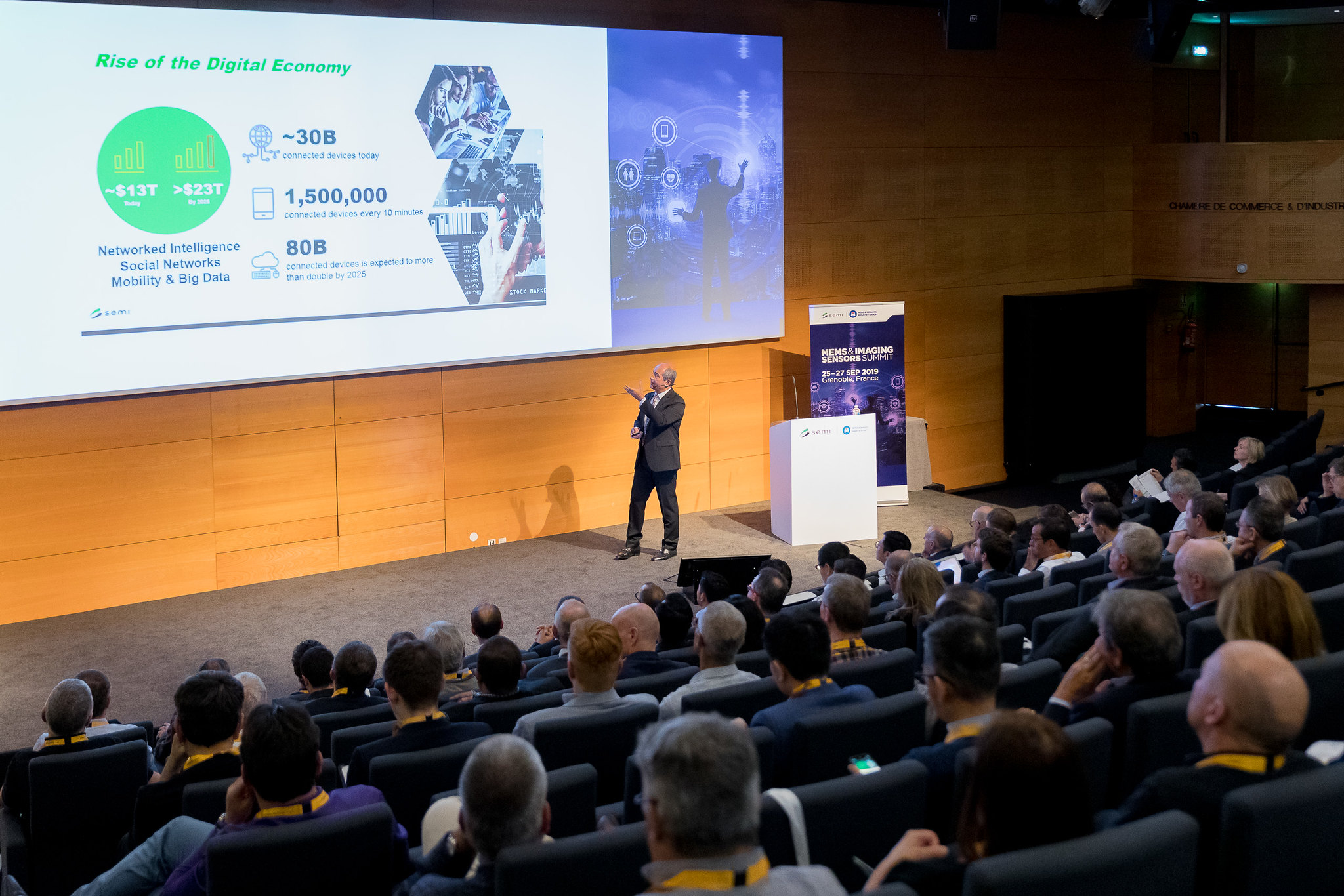
Laith Altimime, president of SEMI Europe, sets the scene for the European MEMS and imaging sensors at the conference in Grenoble
(Image: SEMI)
Alibaba Cloud’s lead solution architect in Europe, Yanchao Wang, talked about a world two decades from now when there will be an IP address for everything, and about the platform Alibaba Cloud has developed along with its AliOS operating system to “create the bridge between physical and digital worlds”. He like others talked about open connection platforms that works with all industry players. The focus for Alibaba, he said, was smart cities, smart manufacturing and smart life — for the latter it already has 50 million devices shipped on its smart life platform.
Avi Strum, senior vice president of the sensors business unit of Tower Jazz talked about the merits of optical fingerprint and 3D face recognition sensors for cellular security applications, and in particular the trend towards use of time of flight (ToF) and direct ToF sensors due mainly to cost. He hinted at rumors in China that Apple might return to using fingerprint recognition as well as facial recognition, adding, “Rumors in China often end up becoming true.” He also said that eventually, phones would use both fingerprint and facial recognition, and that the fingerprint would be optical.
If anyone had doubts about Finland’s ability to build on its radio heritage, they were dispelled in the keynote from Antti Vasara, president and CEO of VTT in Finland. He highlighted the projects and spinouts from VTT, ranging from the first MEMS-based hyperspectral imaging camera, which is already being trialed in nanosatellites, as well as for detecting skin cancer and in agriculture; to their work on terahertz imaging and its deployment in airport security. He also highlighted work in micrometer scale photonics and solid-state lidar, which enables beam steering with no moving parts.
During the two days of the conference, we picked up 10 of the things that we thought worth a mention here to capture a flavor of the talks and the direction of the industry.
MEMS Growing Fast: 8.2% CAGR to 2024
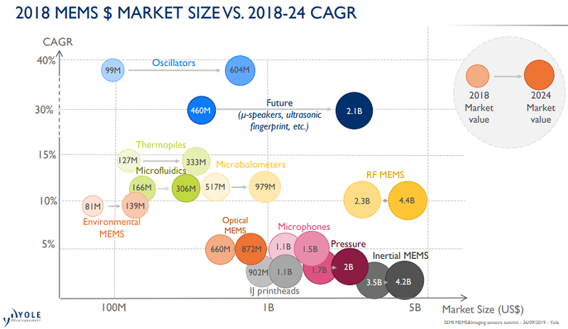
Image: Yole Developpement
The global MEMS market reached $11.6 billion in 2018 and is expected to grow at an 8.2 percent CAGR up to 2024, according to Yole Développement. Consumer applications account for 60 percent of the MEMS market while automotive applications account for 20 percent. The remaining 20 percent include telecom, medical, industrial and aeronautics applications.
“This graph,” Dimitrios Damianos, technology market analyst with Yole, said, “shows three pockets of growth.” The first pocket, whose market value is below 5 percent CAGR, is mostly composed of legacy MEMS (e.g. MEMS microphones, inertial, pressure and optimal MEMS).
The second pocket of growth, between 10 and 15 percent, encompasses environmental MEMS, microfluidics, microbolometers, thermopiles and RF MEMS. For instance, Damianos explained, “thermopiles are used in smart building because of their low-cost availability, microfluidics are used for DNA sequencing, and microbolometers are used as redundant sensors for thermal imaging in ADAS and robot taxis.” And despite a slowdown in the smartphone market, 5G is set to drive the demand for new chips. RF MEMS will indeed be required for the deployment of new base stations and for edge computing.
The last pocket of growth is in the range between 15 and 20 percent, Damianos said. Emerging MEMS such as microspeakers and ultrasonic fingerprints are expected to fuel future market growth. Finally, sensor fusion coupled with AI and edge computing could stimulate new use cases and reinvigorate the MEMS market.
Six Golden Rules for Smart Sensors
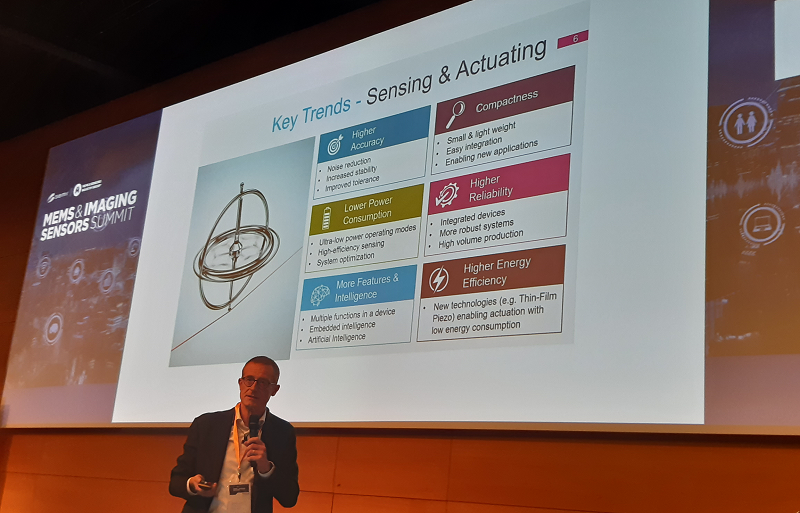
Image: EE Times
The automation age is here. Sensors play a key role in bonding the analog world to the digital world, and their deployment is enabling smarter cities, homes, factories as well as smarter cars and personal devices.
“For the first time, we see two worlds, which never talked to each other, starting to cross the bridge to support new trends such as the industry 4.0,” said Andrea Onetti, analog and MEMS group vice president for the MEMS sensor division, STMicroelectronics. “It is the right timing to have the capabilities to scale up MEMS,” but this will only possible if companies follow these six golden rules: higher accuracy; lower power consumption; compactness; higher reliability; higher energy efficiency; and more intelligence.
Over the past ten years, Onetti said, “We have been able to reduce the power consumption by a factor of 2, the size by 70 percent, and the cost by 75 percent. We have improved the accelerometer noise by 73 percent, the gyroscope temperature stability by 83 percent, as well as increased the full-scale range by 100%.”
Last but not least, “we have been able to insert digital functions that can be processed locally for better efficiency of the overall system.” As sensors give access to more and more accurate, time-relevant, pre-processed data, new business models for hardware makers and service providers will emerge.
Cloud Simulation Surpasses Prototyping for MEMS Development
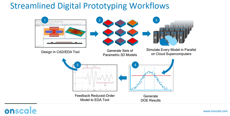
Image: OnScale
Recently, simulation technology, especially cloud simulation, has surpassed the efficiency of physical prototyping. MEMS companies now simulate millions of potential sensor designs to reduce physical prototyping, and eventually lower the cost, risk, and time-to-market. OnScale Inc. (Cupertino, Calif.) is one of them.
Founded in 2018, OnScale claims it combines advanced multiphysics solvers with almost infinite cloud supercomputing capability. “This is giving engineers access to supercomputers in the cloud to run very advanced multiphysics analysis for their MEMS devices,” the startup CEO Ian Campbell said.
“A digital prototype is a representation of a physical device,” said Campbell. “It gives all the engineering data that you would expect from a physical device, but without going through the process of prototyping it, packaging it, simulating it, and finally testing it. So we can tell engineers if their device is going to work, or not, before they go down the very costly process leading to physical prototyping.”
As part of the cloud simulation for MEMS, OnScale executes digital qualification and studies packaging, assembly variability impacts on the overall performance. And, Campbell said, “If you have a MEMS foundry partner or your own foundry, you have process engineers collecting process data. We can use that information and fill it all the way back to the design engineers and also use process simulation to prove foundry yields.”
Spectral Sensing: The Lab-to-Sample Approach
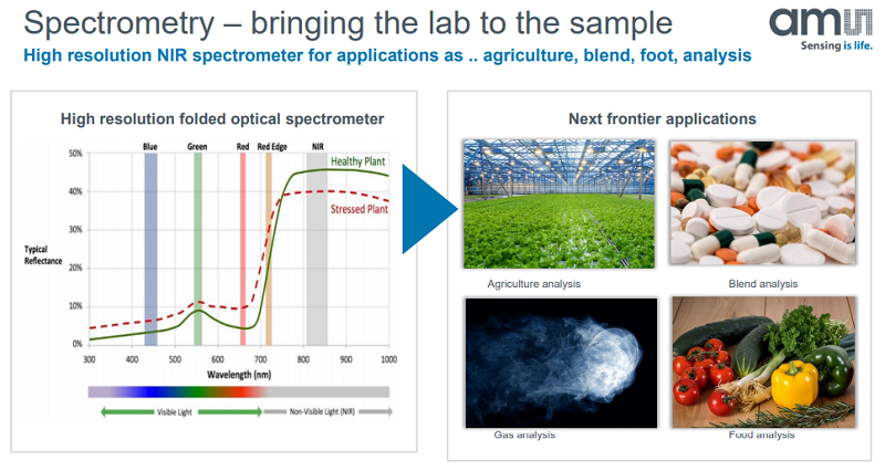
Image: ams
The sustained reduction in the size and cost of spectral analysis enabled by new sensing solutions is taking the lab to the sample. At the MEMS & Imaging Sensor Summit, ams AG showcased optical sensing technologies which are transforming personal health monitoring and smart agriculture.
“Measuring physical parameters on the go drive the demand for miniaturization of spectroscopy,” said Verena Vescoli, senior vice president of R&D, ams. “There is a huge variety of applications for spectral sensing (e.g. color matching, cosmetics skin tone, diagnostics in healthcare, food and agriculture analysis), depending on the wavelength range in which you sense.”
Vescoli mentioned a spectrometric device example based on single-slit folded grating-based optics. “This is consisting of a silicon sensor, but the spectral range is covered by a pure wafer-level optics (WLO) construction.” The above slide shows the spectral footprint of a stressed plant in the wavelength range of 300 to 1000 nm. “You see that the fingerprint or the signal given by the plant can be different,” she explained. “The spectral footprint is even more interesting if you go towards the short wavelength infrared wave, because there you can capture the different overtones of the common oscillations of your molecules.” In other words, she concluded: “The bigger the spectrum is, the better you can catch the fingerprint, and you get a much better signal.”
Okmetic Oy Wins Award for its MEMS Silicon Wafer Manufacturing
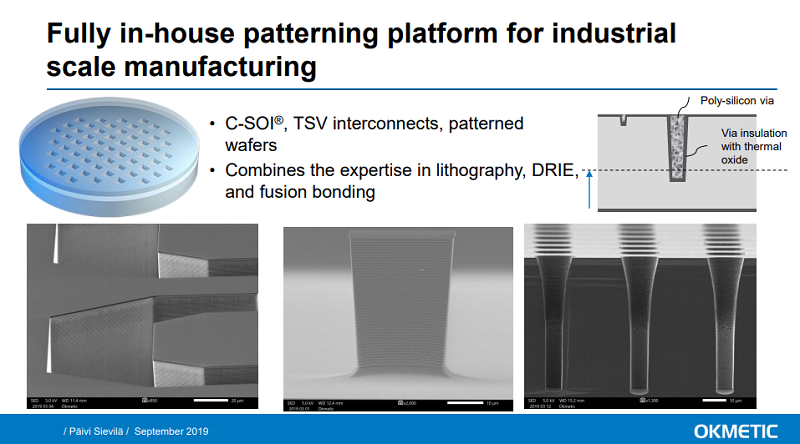
Image: Okmetic
Every year, SEMI’s MEMS & Imaging Sensors Summit awards an innovator of the newest and most unique MEMS and imaging sensors for applications in the industry. This year’s winner is Okmetic Oy, a Finland-based supplier of silicon wafers for MEMS manufacturing, for its recently-launched industrial patterning platform for tailor-made silicon substrate manufacturing.
The platform is designed for MEMS, sensor and photonics applications requiring buried cavities, poly-Si filled through-silicon via connections, or patterned multi-layer SOI design. Explaining the concept, Päivi Sievilä, customer support engineer, Okmetic, said “The crystal properties, the thickness of SOI and the pattern layout can be selected on a case-by-case basis to match what the customers decide. The wafer, or the substrate itself, behaves as a part of a built component from the beginning and streamlines the MEMS process and reduces the device footprint.”
Among the advantages of Okmetic’s crystal growth capability, Sievilä said the silicon properties such as orientation, resistivity and dopants can be adjusted. Also, integrated process scheduling enables reasonable cycle times as the approach decreases handling and transportation between foundries and critical process steps.
Earlier this year, Okmetic expanded its SOI manufacturing capacity to include lithographic patterning and deep reactive-ion etching (DRIE) to enable the production of embedded structures in SOI wafers. The goal is to double the company’s SOI production capacity by the second half of 2020.
Sensors Drive Wearables for Healthcare and Lifestyle
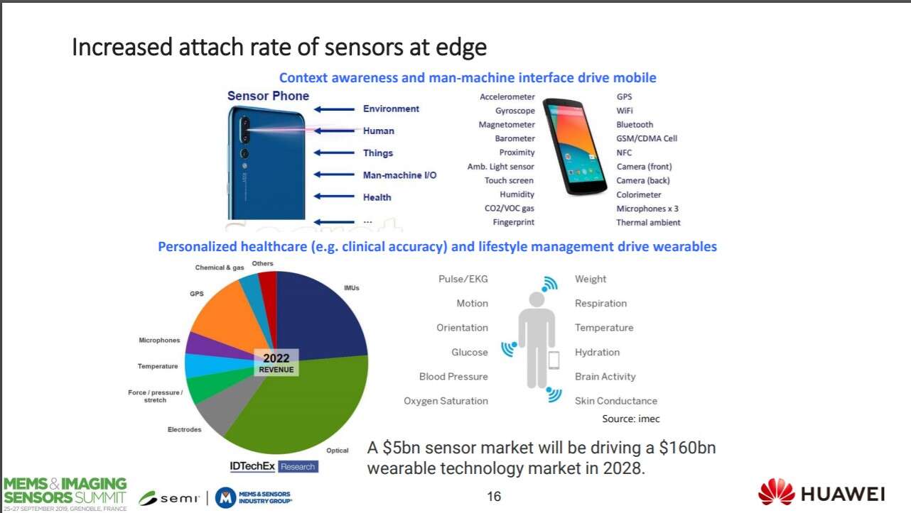
Image: Huawei
The proliferation of sensors will drive wearable devices for both personalized healthcare and lifestyle management. This will ultimately require more intelligence within the sensor. In order to achieve this, Huawei presented the landscape of technologies for enabling more and more intelligent devices, and the new age of heterogeneous computing to drive ‘more than Moore’ computing, or in other words, scale beyond the physical limits of Moore’s Law.
The company’s technical director, Mustafa Badaroglu, said 3D technology gained momentum in 2015, but is now mainstream. Extrapolating forward, we could see memory and logic monolithic integration beyond 2031. He highlighted today’s challenges for mobile — such as how to increase system performance without just relying on clock frequency, and the potential for machine learning and artificial intelligence to become just like general purpose computing is today, bringing large dies to consumer applications.
Environmental sensing came up often at the conference too, enabled by sensors for gas and VOCs (volatile organic compounds), near-infrared, particle monitoring, as well as hyperspectral sensing for food and skin, for example.
PNI Sensor Shows how Smart Parking Generates a Real ROI
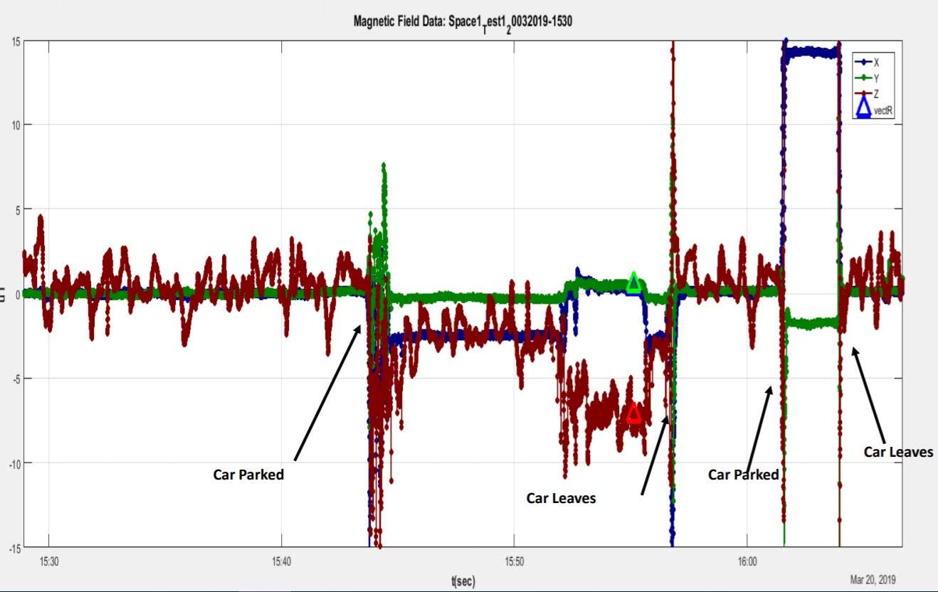
Image: PNI Sensor
PNI Sensor highlighted numerous smart parking applications around the world utilizing its PlacePod vehicle detection sensor, which includes its’ RM3100 geomagnetic sensor, a Bluetooth Low Energy (BLE) module and vehicle detection algorithms. Connected via the LoRa network, it provides continuous vehicle detection ‘without missing a parking event’. The image here grabbed our attention as it identifies the magnetic field signatures for when a car is parked and when it leaves.
Its sensors have been adopted in places like Amritsar, India to minimize illegal parking and increase revenue for parking enforcement; the city of Montreal, to reduce congestion and manage enforcement, operating reliably in extreme cold and snow; in California’s Central Valley to manage parking enforcement; and at Nvidia corporate headquarters, where sensors monitor the availability of spots for special needs, such as EV charging and people with disabilities. In the various public applications, the highlighted cities have seen significant return on investment — for example in Central Valley, 16 PlacePod sensors detected 350 parking violations and generated $10,500 in parking fines.
New Voice Control Devices Demand Audio Specific Architectures
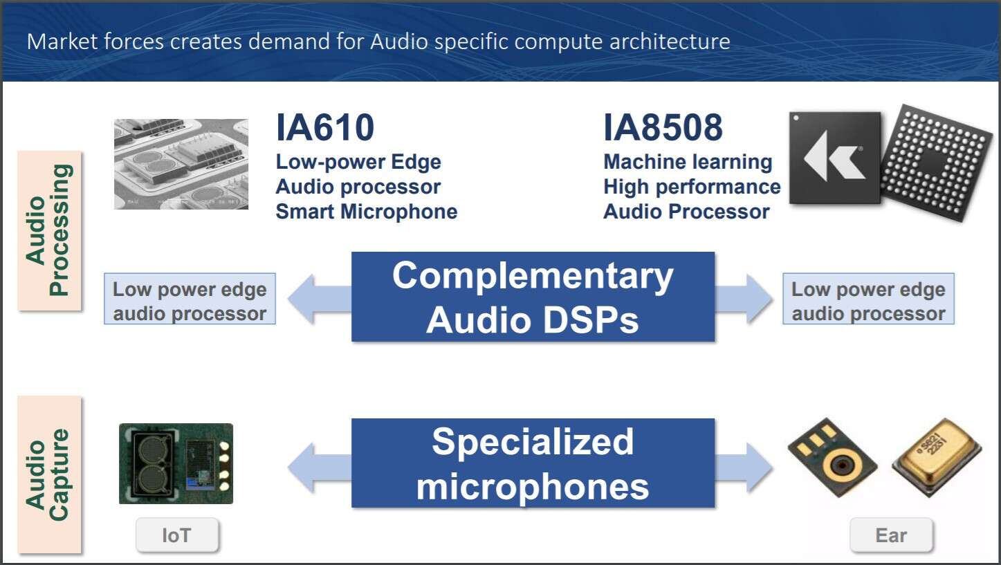
Image: Knowles
A number of presentations at the MEMS and Imaging Sensors Summit focused on new architectures integrating MEMS and lots of processing and artificial intelligence at the sensor, also often called the edge. Knowles, which provides high performance solutions for voice control, talked about the need for domain specific audio processing architectures, very much in the way that GPUs and NPUs have already done for graphics.
Alexis Bernard, chief technology officer for Knowles said the voice user interface is part of a paradigm shift in how people will interact with technology, citing a market of 10 billion installed audio devices in 2020. In his talk, he focused on key requirements for audio-enabled devices — such as advanced sound capture using multiple microphone arrays; advanced audio processing of multiple audio streams using high performance computing; advance machine learning including augmented intelligence and analytics, as well as contextual computing; power efficiency to deal with always-on requirements from tiny batteries; and an open DSP and partner ecosystem.
Earlier this year, Knowles launched its AISonic family of audio edge processors, the IA8201, featuring voice activation and multi-microphone audio processing optimized for power-sensitive applications. Incorporating a high compute 128-bit core (DMX) with Knowles proprietary instruction set and a Tensilica HiFi3 core (HMD), it has the compute power to perform advanced audio output, context awareness and gesture control.
Sub-Retinal Wireless Chip Tackles Vision Loss and Blindness
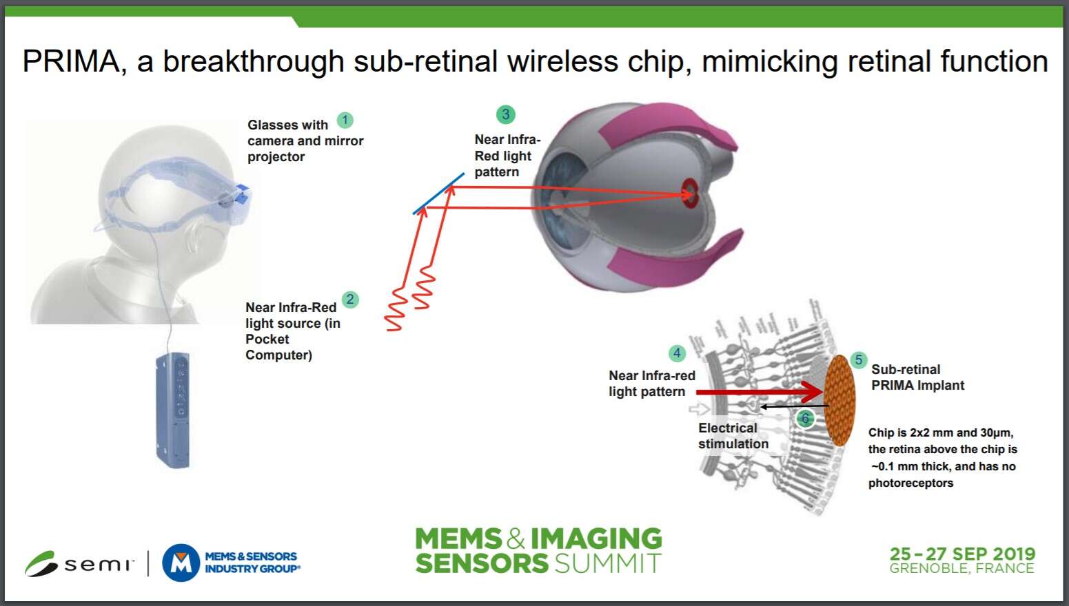
Image: Pixium Vision
Dry age-related macular degeneration (AMD) is a leading cause of severe vision loss and legal blindness in people over the age of 65 in North America and Europe; globally, current projected estimates for people living with AMD is around 196 million people worldwide, and the ageing population means this would only grow.
Pixium Vision presented its sub-retinal wireless chip which can help mimic the retinal function, in effect replacing the degenerated photoreceptors in the eye. Called Prima, its system is said to restore sight in patients with this condition, using a 2x2mm wide 30-micron thick photovoltaic chip containing 378 electrodes. Implanted under the retina via a minimally invasive surgical procedure, it acts like an array of a tiny solar panel powered by pulsed near infrared light projected from a miniature projector transmitting images captured on a mini camera. The camera and projector technologies are integrated into augmented reality glasses, which together with the implant, help patients regain visual perception.
Martin Deterre, engineering manager at Pixium Vision said they have already implanted the bionic eye in five patients in France and have completed a year of clinical study on the implants. Patients had visual rehabilitation, and, at 12-months, most can identify letters with some able to identify sequence of letters and demonstrating increasing speed over time. There were no device-related serious adverse events. He said the company is now working on more transparent glasses incorporating a pocket processor.
Silicon Eye enabling Event-Based Vision
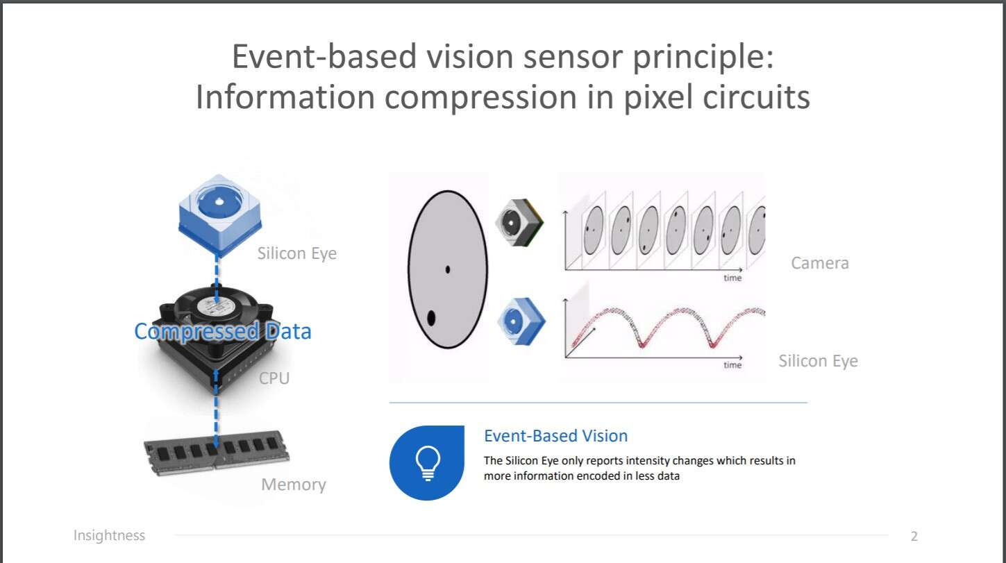
Image: Insightness
Insightness has developed a ‘silicon eye’ using dynamic vision sensors to compress the visual information already in the pixel, resulting in an efficient sensor with low power consumption, fast reaction and high dynamic range. By reporting only intensity changes in received information, it reduces the amount of data that has to be processed.
In collision avoidance systems for drones, the sensors’ high temporal resolution helps overcome the limitations of typical systems which find it difficult to handle dynamic objects. Insightness has integrated its collision avoidance system into configurable modules comprising central processing module which integrates the information from one or multiple conventional or silicon eye vision sensor modules. Depending on the configuration, the system can deliver information like the 3D position of the drone for trajectory control, a depth map to evade static objects and a motion map to evade moving obstacles.
Its SEES2 (an acronym for silicon eye event-based vision sensor) provides a pixel pitch of 7.2µm and 1024 x 768 resolution. It has been built in TPSCo 65nm with pixel-level hybrid bonding. The company is offering evaluation kits of its collision avoidance systems for drone and robot manufacturers and is also now working on a product for augmented reality.

Subscribe to Newsletter

Test Qr code text s ss
