Embedded MRAM Solutions Emerging
Article By : Dylan McGrath, EE Times
Intel, Samsung aiming to join GlobalFoundries in having production-ready tech
SAN FRANCISCO — The world’s two largest semiconductor companies both presented new technologies for embedded MRAM in logic chip manufacturing processes last week at the 64th International Electron Devices Meeting (IEDM) here.
Intel (Santa Clara, California) described the key features of spin-transfer torque (STT)-MRAM–based non-volatile memory into its 22FFL process, calling it “the first FinFET-based MRAM technology.” Describing the technology as “production-ready,” Intel did not name any foundry customers for the process, but multiple sources said that it is already being used in products now shipping.
Samsung (Seoul), meanwhile, described STT — MRAM in a 28-nm FDSOI platform. STT-MRAM is regarded as the best MRAM technology in terms of scalability, shape dependence, and magnetic scalability.
MRAM technology has been in development since the 1990s but has yet to achieve widespread commercial success. “I think it’s time we show something manufacturable and something commercial,” said Yoon Jong Song, a principal engineer in Samsung’s R&D center and the lead author of the company’s IEDM paper.
In addition to being seen as a promising candidate for standalone devices to replace memory chip stalwarts DRAM and NAND flash — which are facing serious scaling challenges as the industry moves to smaller nodes — MRAM, which is a non-volatile memory, is appealing as an embedded technology replacement for flash and embedded SRAM because of its fast read/write times, high endurance, and strong retention. Embedded MRAM is considered especially promising for applications such as internet-of-things (IoT) devices.
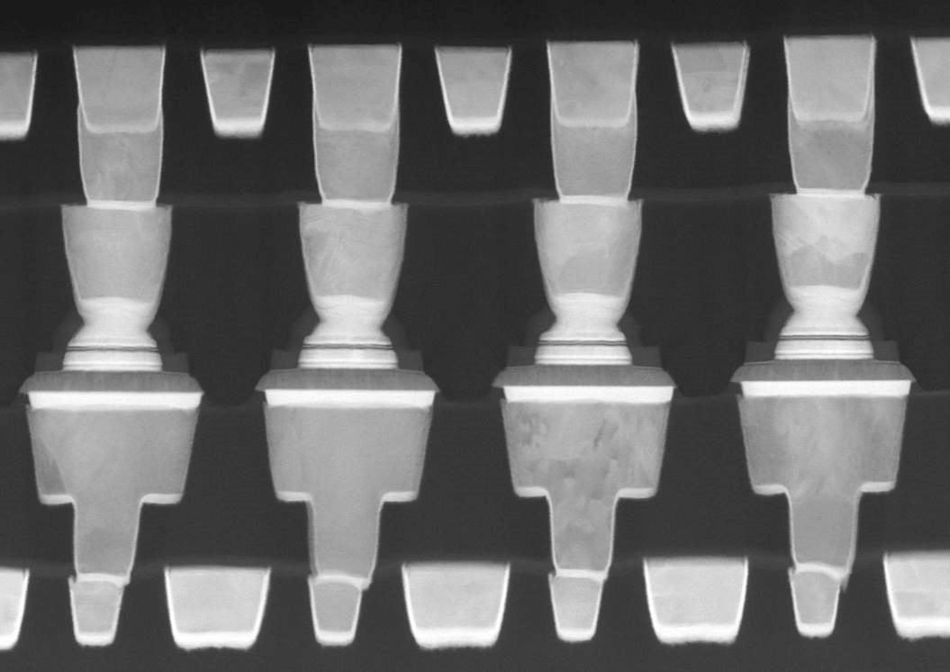
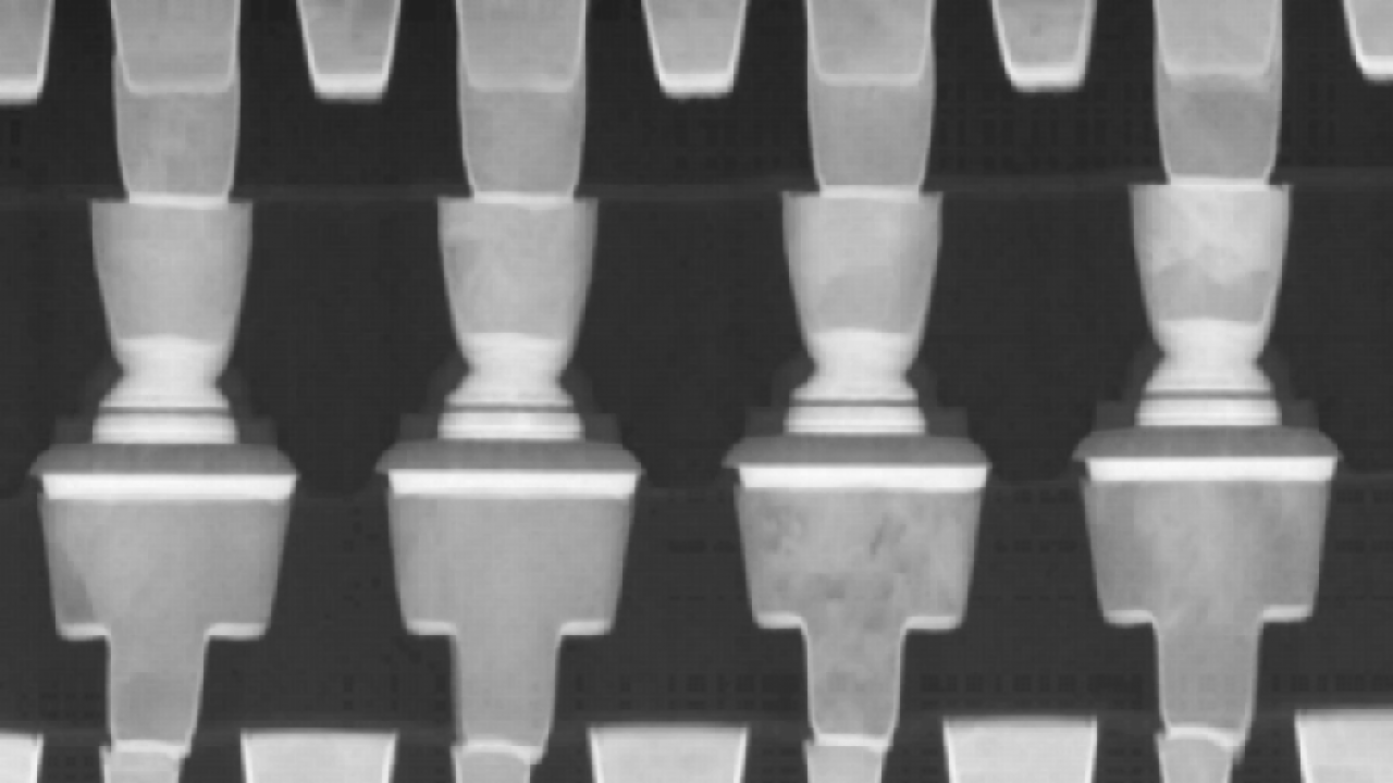
An electron microscope image showing the cross-section of the MTJ array, which is embedded between Metal 2 and Metal 4 in Intel’s 22-nm FinFET logic process. (Source: IEDM/Intel)
Globalfoundries has, since last year, been offering embedded MRAM on its 22FDX 22-nm FD-SOI process. But Jim Handy, principal analyst with Objective Analysis, said that he is not aware of any commercial products shipping the Globalfoundries’ embedded MRAM technology.
“The reason why nobody has picked it up is because of the fact that they would have to add new materials,” he said.
But embedded MRAM is gaining greater consideration as manufacturing costs come down and other memory technologies face scalability challenges. “The big deal is that, with new process technologies, the size of the SRAM cell isn’t shrinking with the rest of the process, so MRAM becomes increasingly appealing,” said Handy.
In its paper, Intel said that its embedded MRAM technology achieves 10-year retention at 200°Celsius and endurance of more than 106 switching cycles. The technology uses a 216 × 225 mm 1T-1R memory cell.
Samsung, meanwhile, described its 8-Mb MRAM with endurance of 106 cycles and retention of 10 years.
Song said that the Samsung technology will be initially available for IoT applications, adding that the reliability has to improve before it can be used in automotive and industrial applications. “We have successfully transferred the technology from lab to fab and will be moving it to market in the near future.”

Subscribe to Newsletter

Test Qr code text s ss
