Deep Inside SK’s 72-Layer NAND
Article By : Jeongdong Choe, Senior Technical Fellow, Techinsights
Senior TechInsights analyst picks apart SK Hynix's 72-layer 256Gb NAND
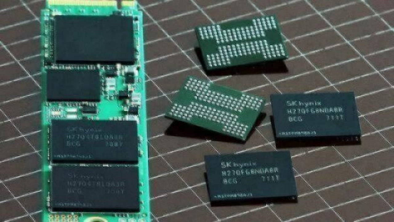
The so-called P-BiCS cells use pipe gates to connect each NAND string. From the floor plan, we can see the die consists of four planes and two-sided wordline switches/decoders.
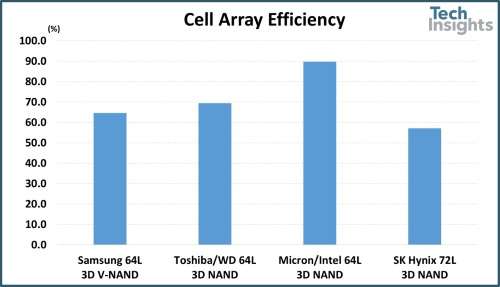
Memory array efficiency is about 57% due to its relatively large memory and other peripherals. SK Hynix 36L and 48L have memory array efficiencies of 67.5% and 64.0%, respectively. The trend suggests SK Hynix likely will develop a more compact design for its next-generation chip.
By comparison, Samsung and Toshiba/Western Digital 64L 3D TLC NAND die have more than 65% memory array efficiency, However, the die sizes and memory capacities are similar to each other.
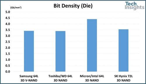
Memory bit density of the SK Hynix 72L NAND is 3.55 Gbits/mm2, higher than figures for the 64L chips from Samsung and Toshiba/Western Digital. The Micron/Intel 64L 3D NAND die offers the highest bit density of the four solutions, due to its unique tile floorplan architecture called CMOS under the array (CuA).
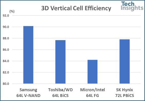
When it comes to the 3D NAND cell structure, SK Hynix chips stack a total of 82 gates, including selectors and dummy wordlines. We know that 72 gates are for active wordline cells and the top-most three gates are for source side and drain side selector gates (SG). The remaining seven gates are likely used for dummy wordlines (DWL) and isolation gates.
Looking at 64L NAND devices:
- Samsung uses 71 total gates–three for SG, four for DWL
- Toshiba/Western Digital use 73 total gates–seven for SG, two for DWL
- Micron/Intel use 76 total gates–two for SG, seven for DWL
Vertical cell efficiency is the number of active wordlines divided by the total number of vertically stacked gates. The result shows the process efficiency of the 3D NAND cell architecture. The vertical cell efficiency of SK Hynix 72L is 87.8%, which is the same as Toshiba and Western Digital’s 64L BiCS. By comparison, Samsung 64L measures 90.1% and Micron/Intel 64L is at 84.2 % as shown below.
SK Hynix’s previous 36 and 48L products used a one-step etching process for the channel holes with 43 and 55 total gates, respectively. The new 72L cell adopts a two-step etching process for the channel holes.
On pipe-gates, the lower 42 gates and the upper 40 gates are formed separately with two different etching steps. Slits and sub-slits are formed by one-step etching. The process integration sequence is as follows:
- Pipe gate mold formation (lower portion)
- Channel etching (lower portion)
- Sacrificial layer filling into holes
- Mold formation (upper portion)
- Channel etching (upper portion)
- Sacrificial layer removal
- Channel formation
Micron/Intel 64L adopted a double-stack NAND string architecture with a plate between upper and lower stacks. By contrast, SK Hynix 72L has a two-step etching process rather than the double-stack NAND string. Engineers must tightly control steps to avoid misalignment of upper and lower channel holes, measured at about 10 nm in the 256 Gbit 72L products.
For more details, see the full analysis online of the SK-Hynix 72L NAND design.
— Jeongdong Choe is a senior technical fellow at TechInsights

Subscribe to Newsletter

Test Qr code text s ss
