TSMC Updates its Silicon Menu
Article By : Rick Merritt, EE Times
TSMC added process and packaging variants to its broad foundry portfolio, but one analyst said some updated results were below projections it made six months ago. First 7nm chips, EUV migration described.
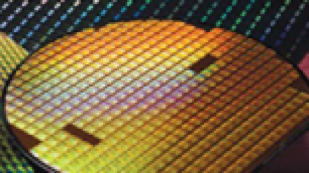
SANTA CLARA, Calif. — TSMC reported progress in 7nm and extreme ultraviolet (EUV) lithography and bolstered a planar process that competes with fully depleted silicon-on-insulator at an annual event here. It also gave updates on its work in packaging and platforms for key market segments.
The foundry, celebrating its 30th anniversary, expects to tape out more than ten 7nm chips this year and start volume production with the process next year. The chips include a quad ARM A72 core processor running at up to 4 GHz — possibly Huawei’s Kiron mobile processor — a CCIX development platform, and an unnamed ARM server processor.
TSMC sketched out what it called a relatively simple process of porting design rules and IP to an N7+ process using EUV it could put into production in 2019. The process can deliver 20 greater greater density, 8-10 percent higher speeds or 15-20 percent less power than its current N7 node. Compared to its 16FFC process, N7+ can enable 30 percent higher speed or 50 percent less power on an ARM A72 core, said Cliff Hou, vice president of R&D for design technology at TSMC.

The foundry will provide a utility to port immersion design rules to the EUV process that will “clean up most of the layout differences,” Hou said. Overall, the work of moving from N7 to N7+ should represent about a third of the effort of migrating to a new node, he added.
TSMC maintains four market-specific platforms with unique process features and IP. The leading-edge process is focused mainly on a high-performance computing platform that supports greater overclocking, lower resistance metal interconnects, tailored caches and libraries. “We make the HPC flow really work for servers,” said Hou.
Targeting chips for the Internet of Things as well as 5G cellular, TSMC added a 22nm ultra-low leakage (ULL) variant to its 22nm ultra-low power (ULP) planar process announced in March. The two processes should be available next year with Spice models ready by the end of 2017 and IP blocks ready in the first quarter of 2018.
The 22ULL process includes analog and RF improvements to serve millimeter wave 5G chips as well as embedded memories optimized for low leakage. It supports parts running at 0.8V and lower voltages for power management ICs. The node could provide a 5 percent optical shrink and lower power by 25 percent compared to designs made in a 28HP+ process.
In between its 7 and 22nm nodes, TSMC is developing a 12FFC process that should be ready for production in 2019 using a new six-track (6T) standard cell library, down from 9- and 7.5T on the 16FFC node. The 12FFC process could shrink area 14-18 percent or provide 5 percent more speed.
[Next page: Some results not up to earlier projections]

Subscribe to Newsletter

Test Qr code text s ss
