TSMC Sees HPC Driving Business
Article By : Junko Yoshida, EE Times

TSMC says that high-performance computing, including demand for chips used in cryptocurrency mining, has replaced smartphones as the key driver of its business.
TAIPEI — Taiwan Semiconductor Manufacturing Co. (TSMC) says that high-performance computing (HPC), including demand for chips used in cryptocurrency mining, has replaced smartphones as the key driver of its business.
While low- and mid-tier smartphones still show signs of growth, sales of leading-edge handsets are likely to be “flat”, according to the world’s largest foundry, which makes all of the application processors used in Apple’s latest iPhones as well as silicon used in handsets from a range of Chinese manufacturers such as Huawei, Oppo and Xiaomi.
HPC, which under TSMC’s definition includes applications for AI, GPUs and cryptocurrency mining, is picking up just as smartphone demand is losing momentum, the company said. While AI ASICs such as those used for cryptocurrency mining may to a degree be eroding sales of GPUs, demand for both types of chips is quite “solid”, according to TSMC.
{image 1}
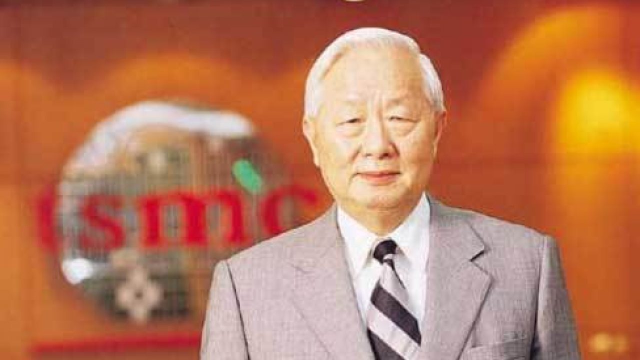
TSMC believes it will continue to lead chip industry growth in 2018 with the company’s annual revenue gaining by as much as 15 percent from the $32 billion in sales recorded in 2017. The overall growth rate for the foundry segment this year will be about 10 percent while the semiconductor industry will grow by as much as 8 percent, according to TSMC Chairman Morris Chang, speaking at an event to announce the company’s fourth-quarter 2017 results.
IDMs Go Fab Light
Contributing to TSMC’s industry-leading growth is a renewed trend toward more outsourcing by IDMs, according to Chang.
“Almost without exception, every IDM has become fab-light,” he said. “Those will become fab lighter and lighter and lighter.”
IDMs now depend almost solely on foundries for support below 90 nm, according to TSMC Co-CEO Mark Liu. Much of the new IDM outsourcing to TSMC will be for automotive semiconductors, he said.
While the company agreed with UBS analyst Bill Lu that foundry supply is becoming tight, TSMC doesn’t plan to increase its capital expenditures for 2018 significantly compared with last year. TSMC said its capex target for this year is $10.9 billion, little changed from the $10.8 billion the company spent in 2017. During the next few years, the company plans to keep capex in a $10.5 billion to $11 billion range.
The company’s latest 10 nm process, which it ramped up in 2017 to make the A11 application processor on a sole source basis for Apple’s latest iPhone X, accounted for 25 percent of TSMC’s revenue during the fourth quarter of last year. The contribution of 10 nm to TSMC’s sales during the first quarter of this year will drop due to the seasonality of the smartphone business, according to TSMC. While some 10 nm customers migrate to 7 nm, the company said it expects sales of 10 nm to grow in 2018 to meet demand for application processors, cellular baseband and ASIC CPUs.
In the meantime, TSMC has continued to enhance its legacy 28 nm/22nm and 16 nm/12 nm nodes with low-power and high-performance tweaks. The company said that in the next few years, 22 nm will play a more important role than the 28 nm process that has been the company’s cash cow for more than five years.
Leading Geometries
TSMC expects to have a 100 percent share of the 7 nm business when it starts production of the new process technology in June this year.
That expectation reflects on Samsung and Qualcomm, according to one analyst.
“This implies Qualcomm is switching back to TSMC for its first 7 nm product ramp,” said independent analyst Andrew Lu in a report for Smartkarma. Samsung may have delayed its 7 nm ramp as a result of its decision to fully implement EUV at the 7 nm node, according to Lu. Qualcomm several years ago switched from TSMC to Samsung as its foundry for Snapdragon processors.
TSMC said it expects to do 10 customer tapeouts on 7 nm during the first quarter and a total of 50 tapeouts during 2018.
Most of TSMC’s initial 7 nm production will go to customers in the smartphone business, followed by those in HPC. The company forecast that 7 nm will account for about 10 percent of its sales during 2018.
Following the introduction of 7 nm, the company will in 2019 introduce its N7+ process, an enhancement of the 7 nm process to include extreme ultraviolet (EUV) lithography at several layers. TSMC expects that N7+ will increase dies per wafer by about 10 percent compared with N7 because of EUV.
TSMC said its 5 nm process is on schedule for risk production in the first quarter of 2019 and that 5 nm customer test chips are running in its fabs.
The company said it is using EUV equipment operating at 160 watts to support TSMC’s 7 nm and 5 nm rollout. EUV scanners with source power at 250 watts have been installed in the company’s fabs, and TSMC said it is confident that EUV will be ready for the introduction of N7+ in 2019 and N5 in 2020.
The company said that even as Moore’s Law loses validity, it is positive about making 3 nm chips in the future using EUV and its chip-on-wafer-on-substrate (CoWoS) packaging technology.
“We are still pathfinding,” said TSMC Chairman Chang. “There was a question on whether it was feasible.”
—Alan Patterson covers the semiconductor industry for EE Times. He is based in Taiwan.
1.
Subscribe to Newsletter
Test Qr code text s ss


