Time for a New Playbook
Article By : Dylan McGrath
Applied Materials' CEO says the innovation required to drive the IC industry will rely on greater collaboration across the entire ecosystem.
In the debate over whether Moore’s Law is alive or dead, Gary Dickerson, president and CEO of semiconductor capital equipment vendor Applied Materials, takes the position of Switzerland.
“There are very passionate arguments on both sides,” Dickerson observed during a keynote address at the recent Semicon West trade show. “I think the key point is that the innovation of the future has to be different. We have to think differently and we have to drive innovation in a very different way.”
Dickerson’s point: Whether the principle of brute-force scaling that has driven the semiconductor industry forward for half a century remains viable is immaterial. Everyone — even those who say that Moore’s Law is alive and well — agrees that scaling alone is no longer enough. Chipmakers need a bigger bag of tricks going forward.
“Whatever we did in the past that enabled this incredible innovation … that’s not going to work for the future,” Dickerson said during a subsequent interview with EE Times. “That has run out of gas. There’s no question.”
The semiconductor manufacturing ecosystem is indeed almost universally aligned on the broad strokes of the future of chip building. In addition to continued scaling, new architectures, device structures, packaging technologies, and materials will fuel the industry’s drive toward greater system performance and power efficiency.
Dickerson considers these to be the five elements of semiconductor manufacturing’s “new playbook.” Because innovation of the future will require not just one knob but several, succeeding with this new playbook is going to require new types of collaboration and new partnerships between companies at previously disparate ends of the manufacturing supply chain and the electronics ecosystem, he said. “With this new playbook, you can’t look backward. People may be nostalgic about what we created in the past, but the future’s not going to look like the past. So I think the companies that can think differently and can connect across the ecosystem better and faster … are the companies that are going to be successful.”
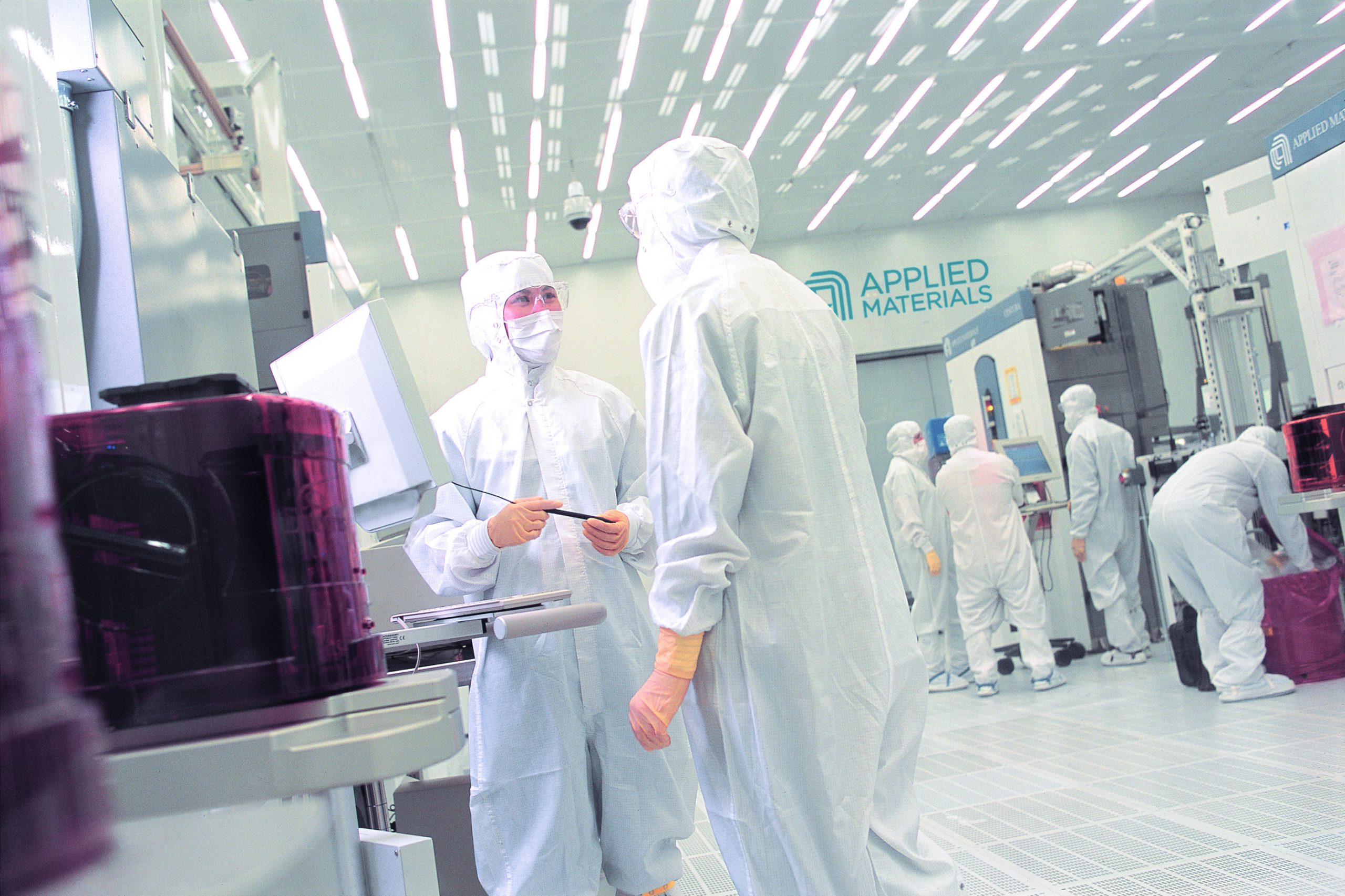
Dickerson speaks from a perspective of hands-on experience in semiconductor manufacturing. Early in his career, he spent six years working in fabs — mostly in lithography — at GM’s Delco Electronics Division and AT&T Technologies. He later worked in a number of areas on the equipment side, spending 18 years in inspection and metrology at chip equipment vendor KLA-Tencor and was CEO of ion implementation fab tool vendor Varian Semiconductor Equipment for seven years prior to its acquisition by Applied in 2011. He was appointed president of Applied in 2012 and CEO of the company in 2013, when he was promoted to replace Mike Splinter.
And when it comes to the importance of connecting with the ecosystem, Dickerson walks the talk. He estimated that he spent about 20 days traveling in June, meeting with Applied customers around Asia, Europe, and the U.S. — including sitting down with the R&D leaders of the company’s top customers in Taiwan, South Korea, and the U.S. “I love interacting with customers and working together to figure out how we drive innovation.”

The point, he emphasized, is the importance of cross-collaboration and a better understanding of what is needed from a chipmaker’s perspective and what is possible from the equipment supplier’s perspective. “I spent many hours with those people really thinking about how we can drive and accelerate innovation. And again, you’ve got to think differently, whether it’s internally within Applied or across the whole ecosystem.”
To help stimulate collaboration between Applied and customers, the company last year announced a new facility in upstate New York, dubbed the Materials Engineering Technology Accelerator (META) Center. The 24,000-square-foot facility, which is set to open later this year, will enable customers to work with new materials and develop new processes on Applied tools.
Difference between lab and fab
Among the big points that Dickerson stresses is the difficulty that chipmakers face in not only creating new processes using new materials for the AI era but refining these processes so that they can be repeatable in the high-volume manufacturing environment of a chip fab. Hardly a week goes by, he noted, that there isn’t a paper published by researchers in a university about novel semiconductor architectures, structures, and materials that suggest the potential for dramatic impact on the semiconductor industry. But while these breakthroughs are impressive, doing something under university research conditions is significantly different than doing it at low cost in high-volume fab conditions.
“In a lab, you can certainly create architectures that work with certain characteristics,” Dickerson said. “But then when you go from the lab to high-volume manufacturing and you want to make billions of those devices — billions of those structures — at high yield, that’s a whole different kettle of fish.”
This, of course, is where Applied comes in. The breadth of the company — which has been No. 1 in semiconductor equipment sales nearly every year for the past three decades — enables Applied to take a more holistic approach to making semiconductor equipment than many of its more narrowly focused rivals, he argues.
For example, during Semicon West, Applied introduced new Endura platforms for physical vapor deposition targeting emerging non-volatile memories that are being used in IoT and cloud-computing applications, including MRAM, ReRAM, and PCRAM. These tools, Dickerson emphasized, feature up to nine deposition chambers integrated under vacuum and are capable of precision deposition and control of multi-component materials being used in these memories. These systems illustrate Applied’s breadth, incorporating deposition, thermal, and imaging technologies from across Applied.
The semiconductor industry is going to need all of these technologies and more going forward. Among the grand challenges of the AI era that Dickerson sounded the alarm on during his keynote is the enormous power consumption potential of AI data centers, particularly for neural-network training and inference. The adoption rate of AI will be limited unless the semiconductor industry can improve the power efficiency of AI accelerators — to the tune of a 1,000× improvement in performance per watt.
“AI is definitely the biggest economic and investment opportunity of our lifetime,” Dickerson said. “But we also face the biggest challenges from an industry perspective to enable the innovation.”

Subscribe to Newsletter

Test Qr code text s ss
