The Simplicity of Driving CoolSiC™ MOSFETs: A Gate Driving Design Guide
Article By : Klaus Sobe, Infineon Technologies
Parasitic turn-on caused by the Miller capacitance is often considered a weak spot of today’s silicon carbide MOSFETs. In order to avoid that effect, gate-drive designs for hard-switching converters are typically implemented with negative turn-off gate voltages. However, is that really needed with CoolSiC™ MOSFETs?
Introduction
A key element of all gate-drive designs is the selection of the gate- voltage levels. With the CoolSiC MOSFET technology, Infineon allows designers to choose a turn-on gate voltage between 18 V and 15 V, and thus configure the switch for highest current-carrying capability or short-circuit ruggedness, respectively. The turn-off gate voltage level, on the other hand, only needs to ensure that the device remains safely turned off. Infineon encourages designers to operate its discrete MOSFETs at 0 V and benefit from a simplification of the gate-drive circuit.
In order to underline that encouragement, this article introduces an easily reproducible approach to characterize the susceptibility of silicon carbide MOSFETs, and presents tests results obtained with discrete CoolSiC™ MOSFETs.
Parasitic turn-on effect
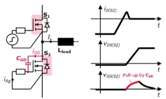
An unwanted turn-on of a semiconductor switch can be caused by inductive as well as capacitive feedback to the gate. In conjunction with silicon carbide MOSFETs, however, it is typically the capacitive feedback via the Miller capacitance that is considered. A scenario explaining this effect is shown in figure 1. The body diode of the low-side switch S2 conducts the load current IL until the high-side switch S1 turns on. After the load current has commutated to S1, the drain-source voltage of S2 starts to increase. During this phase, the rising drain potential pulls up the gate voltage of S2 via the Miller capacitance CGD. The turn-off gate resistor tries to counteract and pull the voltage down. If this resistor value is not low enough to pull the voltage down, the voltage might exceed the threshold level, leading to a shoot-through and an increase of switching losses.
Naturally, the risk and severity of shoot-through events depend on the particular operation conditions and the measurement hardware. The most critical operating points are at high bus voltages, steep voltage rises and high junction temperatures. These conditions not only lead to a stronger pull-up of the gate voltage, but also lower the threshold level. On the hardware side, the major factors of influence are the undesirable parasitic board capacitance parallel to CGD, an external capacitor parallel to CGS, the turn-off gate voltage as well as the turn- off gate resistor.
Characterization setup and approach
Designers often study the gate-charge curve of a specific semicon- ductor switch in order to get an impression of its susceptibility to parasitic turn-on. While this approach is rather straightforward – a brief look into the data sheet is sufficient – it does not really enable conclusions to be drawn for the application. The main shortcoming is that the gate-charge characteristic is rather static in nature, while the parasitic turn-on is clearly a dynamic effect. Hence, dedicated characterization tests are performed to assess the parasitic turn-on behavior of 1200 V/45 mΩ CoolSiC MOSFETs in TO-247 3-pin and 4-pin packages under application conditions. All tests are conducted with a turn-off gate voltage of 0 V.
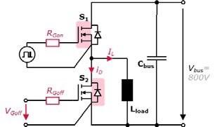
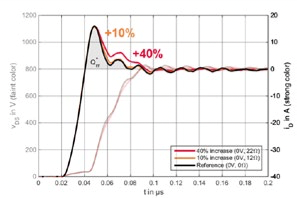
A half-bridge evaluation board is configured as depicted in the schematic drawing of figure 2. It is essentially a commutation cell where the low-side switch is the device under test and the high-side switch acts as dv/dt generator. When the high-side device turns on, the rising drain-source voltage on the low-side device leads to a gate voltage the dvDS/dt, and the lower the turn-off gate resistance, the lower is the chance of a parasitic turn-on. The goal of the experiment is to identify the critical turn-off gate resistance values for a given test case. This so-called critical gate resistance is the value that causes a Q*rr increase of 10 percent compared to the reference waveform obtained with 0 Ω. A threshold level of 10 percent is large enough to get reliable measurement data, but small enough to be considered negligible in most applications, cf. figure 3.
Tests are carried out at different temperatures, different load currents and different voltage slopes. The latter are adjusted using the RGon of the high-side switch S1.
Characterization results
Testing at zero load current means that the body diode of the device under tests is not forward biased prior to the switching transient. No diode recovery occurs; the transient is merely a charging and discharging of capacitances. In this condition, voltages induced in parasitic inductances do not play a significant role. Consequently, also the performance of the TO-247 and the TO-247-4-pin package is the same.
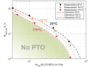
The measurement results obtained at 800 V and 0 A are summarized in figure 4. It is clearly visible that in order to prevent parasitic turn-on, the RGoff needs to be lower, the higher the dvDS/dt and the higher the temperature. It is worth mentioning that a turn-off gate voltage of 0 V is sufficient to prevent parasitic turn-on even at 50 V/ns and 175°C. In case the RGoff cannot be selected at a level that is low enough, drivers with an active Miller-clamp functionality such as the 1EDC30I12MH provide a way out.
At higher load current levels, a hard commutation from the body diode of S2 to the MOS channel of S1 occurs. Due to the presence of diode reverse recovery and induced voltages, the situation becomes slightly more complicated. Simply speaking, three effects come into play:
- The body diode recovery slows down the average dvDS/dt and relaxes the situation with parasitic turn-on.
- Oscillations between the commutation loop inductance and the device output capacitance increase the dvDS/dt locally and make the situation more critical.
- Assuming a standard TO-247 package, the negative feedback via the common source terminal of S2 leads to a reduction of the gate voltage, and thus to an increased ruggedness against parasitic turn-on.
Apparently, the weighting of the effects described above depends on the actual hardware setup. With the evaluation board that was used for all tests presented in this article, the most critical condition is 175°C and 0 A. Thus, the area that is free of parasitic turn-on highlighted in figure 4 holds for 40 A measurements, too – regardless of whether the TO-247 or TO-247-4-pin is considered.
Implications on high-speed switching applications
As indicated in figure 3, the shoot-through current caused by the capacitive turn-on and the reverse-recovery current of the body diode are difficult to differentiate. Both effects slow down or smooth the volt- age transient, and cause an increase of the switching energies, not only on the diode but also on the switch. In applications that require highest switching speeds, parasitic turn-on limits the performance similar to an improper freewheeling diode.
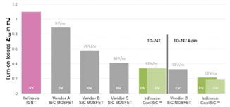
Figure 5 shows the minimum achievable turn-on switching losses of various silicon carbide MOSFET technologies operated with 18/0 V on the gate. While not all devices are able to maintain their high-speed switching nature at such a driving condition, the results confirm the high immunity of CoolSiC MOSFET against parasitic turn-on.
Summary and conclusion
This article describes a simple approach for characterizing the susceptibility of a power semiconductor switch to parasitic turn-on via the Miller capacitance. Test results obtained with discrete CoolSiC MOSFET operated at a bus voltage of 800 V and a switching speed of 50 V/ns demonstrate that even in high-speed, two-level converters, a turn-off gate voltage of 0 V is feasible. When looking at three-level circuits where the switched voltage is just half the bus voltage, the situation eases entirely. In such cases, CoolSiC MOSFET are virtually free of capacitive turn-on, regardless of the gate resistance value.
Assuming a carefully designed PCB layout with minimized gate-drain capacitance, Infineon encourages power electronic engineers to operate discrete CoolSiC MOSFET with a turn-off gate voltage of 0 V. This leads to a simplification of the gate-drive design without penalizing the performance.
For the information on Infineon CoolSiC™ MOSFET, pls visit: https://www.infineon.com/cms/en/product/power/mosfet/silicon-carbide/discretes/
Subscribe to Newsletter
Test Qr code text s ss


