PFIB system offers 20x faster milling rates
Article By : Thermo Fisher
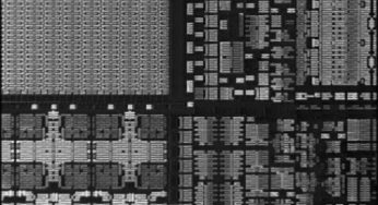
The Helios G4 PFIB system allows engineers to create larger samples for nanoprobing and TEM imaging.
Thermo Fisher Scientific Inc. has announced the Helios G4 plasma focused ion beam (FIB) system designed to deprocess and provide ultra-high-resolution scanning electron microscope (SEM) analysis on a wide variety of semiconductor devices.
The Helios G4 PFIB system can support deprocessing down to the 7nm node and offers automated endpointing that stops milling automatically when the metal or via layer of interest is exposed. According to Thermo Fisher, the PFIB system provides up to 10–20 times faster milling rates than conventional (Ga+) FIB solutions, allowing engineers to create larger samples for nanoprobing and transmission electron microscope (TEM) imaging, as well as large area SEM cross-sections, on a range of advanced (2.5D) packaging, light-emitting diode (LED), display and microelectromechanical systems (MEMS).
Included in the Helios G4 PFIB family are the Helios G4 PFIB HXe DualBeam, Helios G4 PFIB UXe and Helios G4 PFIB CXe systems.
The Helios G4 PFIB HXe DualBeam enables damage-free delayering of 10nm semiconductor devices and advanced failure analysis of 3D packages. The Helios G4 PFIB UXe DualBeam system combines the Elstar electron column with UC+ technology for high-resolution, sub 500eV imaging and endpointing with the high-performance PFIB 2.0 Xenon plasma ion column, for fast, precise, and damage-free large area sample cross-sectioning and deprocessing. While the Helios G4 PFIB CXe DualBeam system is used in sample preparation and analysis of advanced packaging materials.
Thermo Fisher has demonstrated the Helios G4 PFIB system at the 24th International Symposium on the Physical and Failure Analysis of Integrated Circuits (IPFA 2017).

Subscribe to Newsletter

Test Qr code text s ss
