Open Source Initiative Outlines Interfaces and Issues
Article By : Rick Merritt

A group of mainly small- and medium-sized vendors took its first steps toward building a standard for semiconductors assembled from chiplets.
SAN JOSE, Calif. – A group claiming members from 53 companies held its first workshop on creating an open standard for chiplets for accelerators. They aim to enable a low-cost alternative to SoCs at a time when the pace of advancing semiconductors is slowing.
The Open Domain-Specific Architecture (ODSA) group is working under the umbrella of the Open Compute Project, founded by Facebook, that recently announced its first open-source silicon project. It faces steep technical and business hurdles getting market traction, and it’s not yet clear whether it will get the broad participation its ambitions require.
To date, individual companies have made early efforts in creating their own chiplet ecosystems including Marvell’s MoChi, Intel’s EMIB and an offering from startup zGlue. Last summer, Intel released as open source the AIB protocol for its EMIB package as part of its work in a DARPA research program on chiplets.
Chiplets represent one of several efforts to compensate for slowing gains in silicon process technology. They have their roots in multi-chip modules, born in the 1970s, and more recently revived as a cost-saving technique in products such as AMD’s Ryzen and Epyc x86 processors.
“Today all multichip interfaces are proprietary. What we want as a group is to make an open interface, so you can assemble a best-of-breed chip,” said Bapi Vinnakota, an engineer at Netronome, an ODSA founder that aims to offer to the group the RTL for the 800 Gbits/second fabric used in its multicore network processors.
As a start, other ODSA members proposed at the workshop a simple “bunch of wires” as an initial physical-layer interface. It could be run on organic substrates at selectable rates of 1, 2, or 4 Gbits/second/pin.
Future interfaces could include CCIX, 112G and 56G serdes and the RISC-V TileLink. The group proposed using the PCIe PIPE abstraction layer to enable a variety of protocols and PHYs in the future. While its membership is mainly focused on the data center, ODSA ultimately aims to enable chips for mobile and edge systems, too.
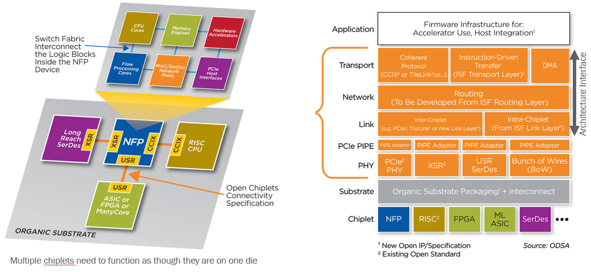
ODSA aims to create a quick proof-of-concept around PCIe while it defines its interface. (Source: ODSA)
The group will support a mix of coherent and non-coherent memory links and could enable bi-directional traffic as a turbo mode. It appears to have rejected Intel’s AIB protocol as too limited in data rates and pinouts.
ODSA plans to create a proof-of-concept based on PCIe before the end of the year. In tandem it will flesh out its PHY, protocol and other specs, suggesting engineers could start work on commercial implementations next year.
The group also aims to define a business flow for chiplets. It will articulate value propositions for different industry segments and define a test certification for known good die, said Sam Fuller, a marketing director at NXP, another ODSA founder. ODSA also needs to attract several key players including packaging vendors, he added.
Other active members include FPGA vendor Achronix that is overseeing the proof-of-concept and On Semiconductor which is providing perspective on power and thermal issues. Startups Kandou, SiFive and zGlue are also co-founders.
About 70 people attended the inaugural event, including about 20 on a livestream. “Every two or three weeks we get four or five new smart people involved,” said Vinnakota of the group that started in October with seven companies.
Samsung, Facebook make the case for chiplets
Samsung showed its support to ODSA, starting off a day of talks at the event it hosted in its North America headquarters here.
“We are figuring out what our chiplet strategy will be, but my personal view is I see tons of interest in chiplets,” said Craig Orr, a senior director of strategy in the Americas for Samsung Electronics.
“I’ve seen lots of companies doing exotic things from 3D stacking to stitching together the largest cuts you can make from a wafer. A lot of networking companies are separating I/O die so today’s serdes can switch to silicon photonics in the future,” he said.
With costs rising, “at the leading-edge nodes there are fewer companies making chips, so if we can lower costs with chiplets we could see more customers,” he added.
For Facebook and other giant data centers, defining silicon is the next big leap after defining a host of systems, boards and modules. With chip thermals rising to the point they see broad use of costly liquid cooling on the horizon, they are under pressure.
A group that includes AMD, Intel, Nvidia, Qualcomm, Xilinx and AI startups Graphcore and Habana joined with Facebook to define a module the size of a large coffee mug to cool high-end chips. The so-called OCP Accelerator Module (OAM) aims to pack up to eight chips running at up to 450W each in air-cooled systems and as much as 700W in liquid-cooled ones.
The module initially targeted performance-hungry AI training jobs. Now Facebook believes it will be used for inference systems as well,
“We defined a 700W option because some companies are thinking about it,” said Whitney Zhao, a hardware engineer at Facebook, citing Nvidia research with a university on multi-die GPUs.
“450W is the line [beyond which] cooling [issues] could impact us a lot. Liquid cooling has a huge impact for the data center. We need time to build that infrastructure — it’s one of our key topics now,” she said.
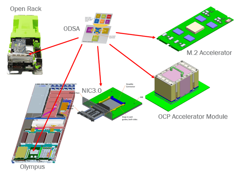
Open Compute members already use a variety of systems for accelerators. (Source: ODSA)
Meanwhile, the OAM is one of at least five system form factors Facebook and Microsoft are using in their data centers, and more are coming. Facebook and partners will start this year defining a universal baseboard, chassis and tray for the new module.
“We need an open accelerator infrastructure,” Zhao said, adding she came to the ODSA meeting to learn about chip-level options.
For chip vendors, the growing variety of systems targets is “an eye opener that our landing zone is a menu of places,” said Vinnakota of Netronome
“We have to decide which of these modules to target and work backwards on what products to use. The short answer is we don’t have a clear idea and will take any help we can get on figuring it out,” he added.

Subscribe to Newsletter

Test Qr code text s ss
