OFC 2020: The Future of Silicon Photonics and Optics
Article By : Nitin Dahad
OFC 2020 went ahead with a combo of live and virtual events to explore the future of optics and silicon photonics engines to address high performance network switching up to 51.2Tbps.
Of the few events that survived the current wave of cancelled events, the OFC 2020 conference and exhibition took place in San Diego, California this week, exploring the future of optics communications and 5G innovations.
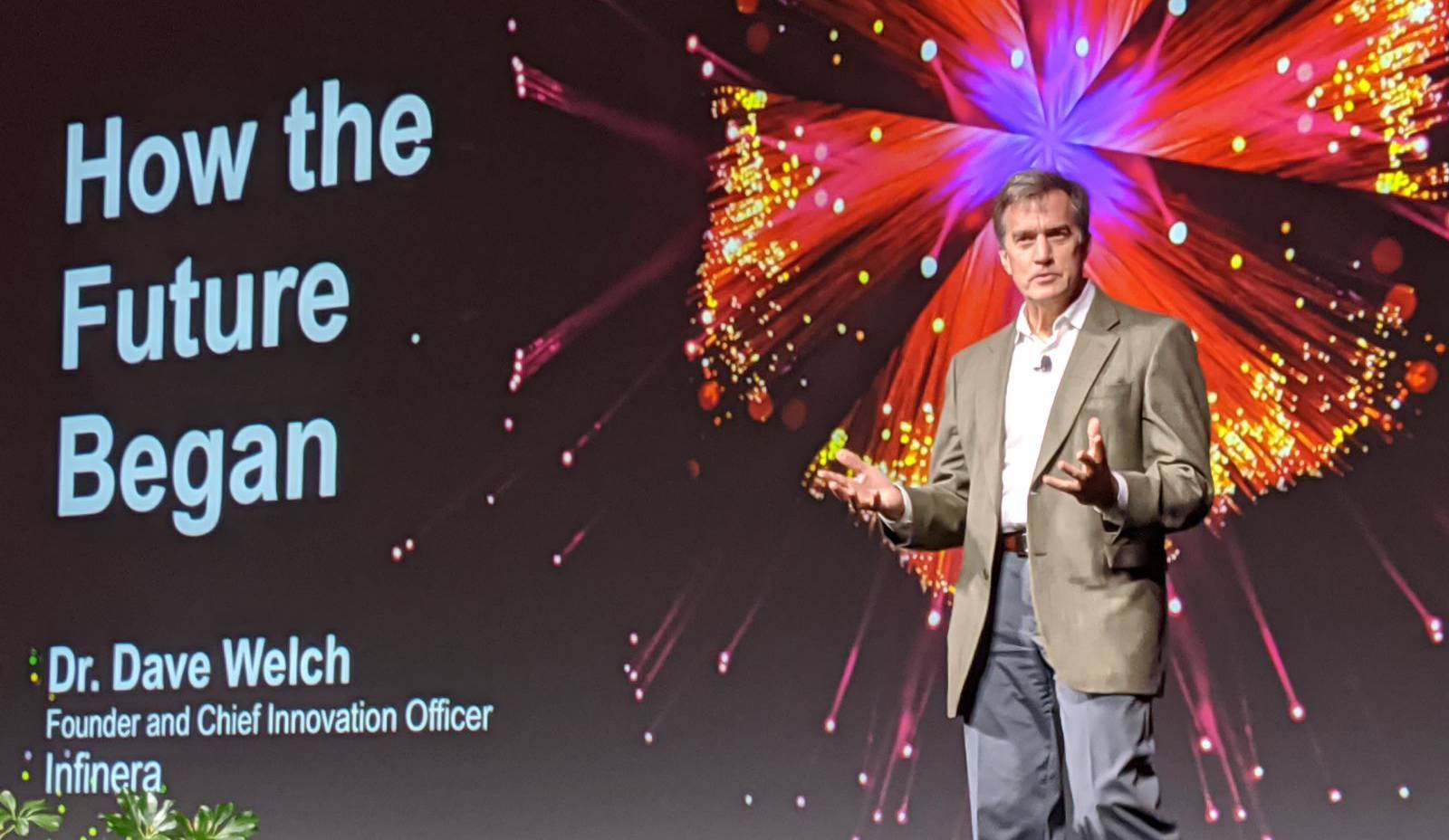
In his keynote address, David Welch, founder and chief innovation officer of Infinera Corp., observed, “Optical networks are central to global connectivity and global communication, and it has absolutely transformed our society and our world. In the end, life is about human-to-human activity. We may elect to utilize machines to facilitate better human-to-human connectivity, and I think that is the greatest contribution of the optical network: the expanse of our human-to-human connectivity.”
Meanwhile, in his presentation, Sir David Payne, director of the optoelectronics research center, University of Southampton, U.K, asked, “Is there a future for silica as an optical material?” He discussed the opportunities for photonics and the need for understanding that photonics is at a crucial time of change. He examined the question of what opportunities are next for photonics research and the markets that could utilize photonics, such as lidar, which is important for the sustained development of driverless vehicles, data storage, and optical data centers.
Payne said, “Materials are incredibly important in photonics, such as the very first silica low-loss fiber, and we now have a wide range of materials and the challenge becomes how to integrate these together in a cost-effective way.” Advances in optical losses, further integration, and quantum applications are key points that Payne believes the OFC community can tackle in the future.
Co-packaged optics and Ethernet switch ICs
One of the big topics is how to address the unprecedented growth of data center traffic with a networking infrastructure that can scale in capacity while maintaining total power consumption and footprint. Today’s disaggregated Ethernet switch IC and optical module architecture does not provide the scalability required to support the future growth of the data centers. Co-packaging of optics and Ethernet switch ICs is a natural next step to reduce the power consumption burden of the electrical I/Os in the data center networking equipment. The transition of the Ethernet switch IC SerDes from 50Gbps to 100Gbps, in 25.6Tbps and 51.2Tbps switch configurations, presents a unique inflection point in the architecture of the Ethernet switch systems.
We covered an approach by Intel earlier this week, but this wasn’t the only announcement in town for high-performance Ethernet networks. Others included Ranovus, which announced a strategic collaboration with IBM, TE Connectivity and Senko Advanced Components, to create an ecosystem to design and manufacture multi-vendor solutions for co-packaged optics applications in data centers, based on its recently announced Odin silicon photonics engine. And Rockley Photonics announced a collaboration with Accton, Molex, TE Connectivity and other industry partners to develop a 25.6T OptoASIC switch system co-packaged with Rockley’s LightDriver optical engine and copper cable attached 400G modules.
Ranovus claims twice the capacity of other solutions
According to Ranovus, its co-packaged optics switch approach in Odin only has twice the capacity of the Intel approach. The Odin 100 Gbps silicon photonics engine, which scales from 800 Gbps to 3.2 Tbps in a single chip supporting both module and co-packaged optics solutions, incorporates the company’s multi-wavelength quantum dot laser (QDL), 100 Gbps silicon photonics based micro ring resonator modulators and photodetectors, 100 Gbps driver, 100Gbps TIA and control integrated circuits supported by a tier 1 packaging ecosystem. The company said the Odin platform delivers 50 percent power consumption/Gbps reduction and 75 percent cost/Gbps reduction over today’s solutions.
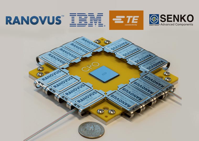
Ranovus’ collaboration with IBM, TE and Senko makes use of IBM’s fiber V-groove interconnect packaging technology, an assembly technique for interfacing optical fibers to silicon photonics devices. The process makes use of passive alignment techniques and achieves low insertion loss across a wide spectral range in both the O-band and C-band regimes. The solution is scalable in physical channel count and the automated process provides a path to high-volume manufacturing of co-packaged optics.
With TE’s co-packaged (CP) fine pitch socket interposer technology, it enables integration of small chipset and optical engine component technologies into high-value co-package assemblies with reworkable and interoperable interfaces. The signal integrity performance of the CP fine pitch socket interposer technology can be critical to 100 Gbps high density electrical packaging requirements. The integration of TE’s thermal bridge technology completes the assembly by providing an innovative solution for thermal management of the switch, SerDes, and optics necessary for high reliability and long operating life.
The Senko fiber optic connectivity solution provides optical coupling, on-board/mid-board, and faceplate to support 100Gbps/lane and beyond co-packaged optics equipment designs. These include low profile and precision fiber coupler assemblies, micro sized on-/mid-board connectors, reflow compatible connector assemblies, and space saving connector options for faceplate.
Rockley silicon photonics scales to 51.2T
Rockley Photonics was one of the few companies that actually attended OFC 2020 to demonstrate its in-package 25.6Tbps optics platform. The company announced a collaboration with Accton, Molex, TE Connectivity and other industry partners to develop a 25.6T OptoASIC switch system co-packaged with Rockley’s LightDriver optical engine and copper cable attached 400G modules.
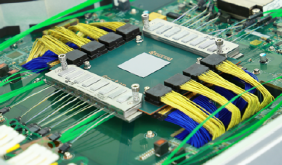
This optical engine is developed using Rockley’s silicon photonics platform enabling 3D integration of electronic and photonic components. It claims to deliver 40 percent savings in power and 60 percent savings in cost compared to transceiver-based optics, and the technology is scalable from 0.8T to 3.2T, allowing Rockley to address system solutions from 25.6T to 51.2T using 100G PAM4 signaling.
Andrew Rickman, chief executive, Rockley Photonics, said, “For co-packaged optics to become a reality it will take a strong and collaborative ecosystem. The partnership demonstrated by Rockley, Accton, Molex and TE we believe is a significant stepping-stone towards delivering high performance and cost-effective optics for hyperscale data center connectivity.”
Accton, a designer of open hardware platforms for data centers, cooperated with several companies to demonstrate the 25.6T co-packaged OptoASIC switch system at OFC2020. The switch system integrates an 800G optical engine via TE’s fine pitch CP socket technology and is also compliant with conventional 400G FR4 QSFP-DD modules through electrical pluggable interfaces. The switch system incorporates Molex’s BiPass/TGA and Samtec’s Si-Fly copper solutions. Accton has integrated the MAC ASIC, optical engine, and copper connectors within a Kyocera substrate, which is connected by an XLA socket from TE Connectivity. Additionally, the demonstration switch platform introduces Vicor’s vertical power GCM device.

Subscribe to Newsletter

Test Qr code text s ss
