IBM: Copper Interconnects Here to Stay
Article By : R. Colin Johnson, EE Times
Copper will serve as the interconnect technology for CMOS forever, no matter how small its feature sizes evolve, according to Big Blue.
LAKE WALES, Fla. — When aluminum interconnects became too slow for complementary metal oxide semiconductors (CMOS) at the 180 nanometer node, IBM led the way to the now universally used copper interconnects starting in 1997.
Now, on its 20th anniversary, many other interconnects are being proposed to replace copper, notably graphene. IBM, however, claims that slight tweaks to copper deposition will give it an enduring edge all the way to the end of the road for CMOS.
Big Blue is touting “copper forever” at the IEEE Nanotechnology Symposium this week in Albany, with more details expected to be revealed at the IEEE International Electronic Devices Meeting (IEDM) in San Francisco.
“Graphene is not readily manufacturable, and furthermore end-to-end comparisons show graphene does not flow uniformly and can’t achieve the low resistances of enhanced copper interconnects,” IBM Fellow Dan Edelstein told EE Times in an exclusive preview of his Nanotechnology Symposium talk.

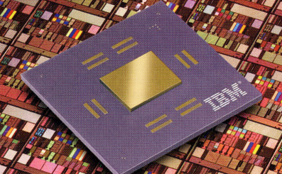
Source: IBM
“Copper with a thin cap of cobalt is better than graphene at carrying current and even at the smallest sizes imaginable copper interconnects are still the best solution, perhaps with cobalt, nickel, ruthenium or another platinum-group noble metals brought in to underlay it,” Edelstein said.
Initial IBM studies showed that copper had 40 percent less resistance than aluminum, resulting in an immediate 15 percent burst in processor speeds. Plus, copper is more durable and 100 times more reliable, according to IBM.
But the industry in the 1990s expressed two big resistances to the changeover to copper — both surmounted by IBM. The first was the fact that copper “poisons” silicon when it comes into direct contact. That was solved by encasing copper in tantalum-nitride and tantalum in a diffusion barrier all around.

The second was its deposition method. Aluminum was previously fabricated as interconnects by depositing an even layer on a topping of dielectric with vias down to the silicon, after which it was etched. Since copper had to be encased in the tantalum compound, this substrative method was not possible. Instead, IBM came up with an additive method with the kind of electroplating used for printed-circuit boards (PCBs).
Electroplating had never before been used on CMOS chips, so stumped the rest of the industry until IBM shared its discovery of it and the encasing process to prevent copper poisoning of the underlying CMOS circuitry. The most complicated part of the process, however, was the dual-damascene process of electroplating inside deep trenches, enabling from seven to 17 (then and today, respectively) metal layers to interconnect the single layer of silicon transistors on typical planar chip. And then there was the “magic.”

Subscribe to Newsletter

Test Qr code text s ss
