Huawei, Apple Use TSMC But Their 7nm SoCs Are Different
Article By : Illumi Huang
Most SoCs in 2019 use 7nm process technologies. But at a closer look, everyone’s 7nm – used in smartphone SoCs or even PC CPUs – seems somewhat different.
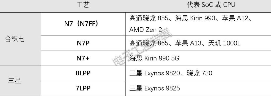
When talking about the most advanced semiconductor manufacturing processes, it seems that most of the SoCs in 2019 can be collectively classified as 7nm. But not all 7nm is equal. We summarize some of the more popular SoCs today. The process used by these SoCs is as follows:
Even if it is 7nm, it seems that there are some differences, and there are even 8nm solutions like the ones offered by Samsung that are only “inferior” by 1nm. These are still worth studying. We also hope that by roughly explaining the differences in parameters of various 7nm processes, we can see what kind of market promotion paradigm each of the current process is using.
A deeper understanding of different 7nm and 8nm processes will also help us understand what these numbers actually mean, and what pace these transistors behind Moore’s Law are now moving forward.
Snapdragon 855 has two 7nm?
TSMC started mass production of the 7nm process in April 2018. In TSMC’s plan, 7nm is a relatively long-term, complete process node. The previous generation was 16nm. The 10nm here is a short-term transition plan. The earliest batch of TSMC 7nm solutions is N7 (or N7FF) in the table above. It is widely used in SoC products such as Qualcomm Snapdragon 855, Huawei Kirin 990, and AMD Zen 2.
TSMC claims that compared to 16nm technology, 7nm has a speed increase of about 35-40%, or a reduction of 65% in power consumption. But this value should be difficult to achieve in real SoCs.
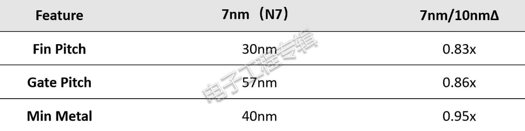
TSMC’s N7 still uses deep ultraviolet (DUV) 193nm immersion argon fluoride (ArF) lithography, which is very different from Samsung’s 7nm low power plus (7LPP). N7 process transistor gate pitch has been reduced to 57nm, interconnect pitch (minimum metal pitch MMP, M1 pitch) is 40nm. Comparing the gate pitch and interconnect pitch with the previous generation and Intel’s process, it roughly looks like as follows:
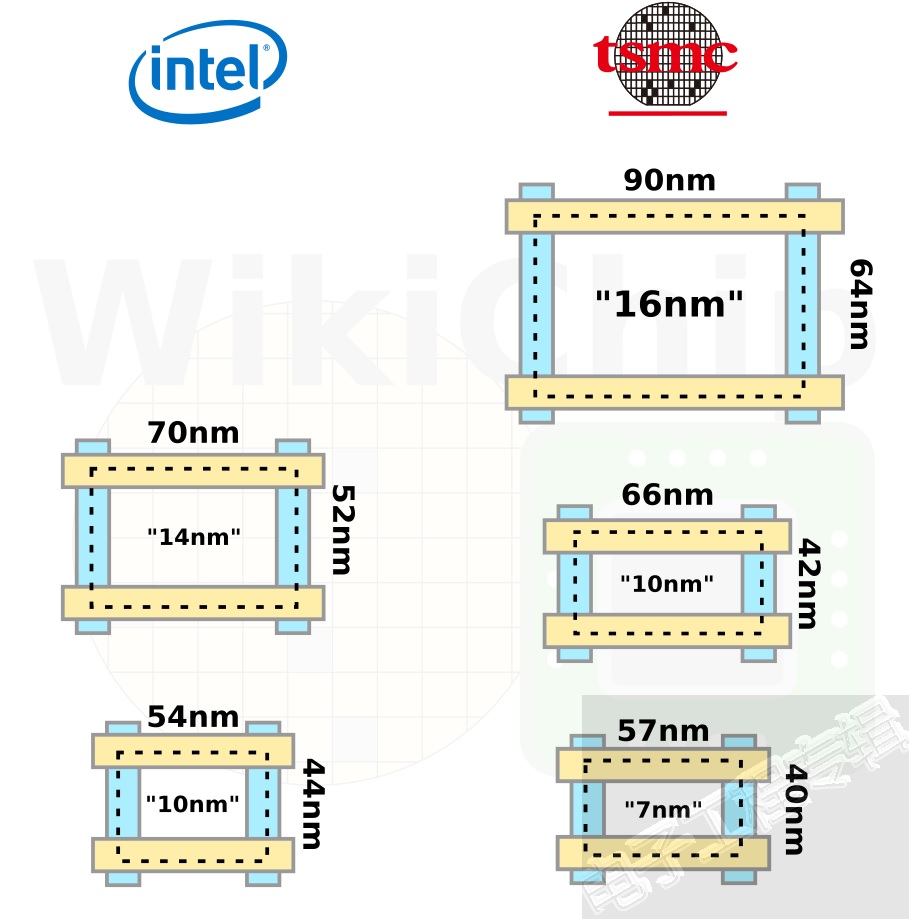
It should be noted that the above data comes from WikiChip. This data actually differs slightly from the official data provided by various manufacturers and seems to be different from the data actually given by other tech research firms such as TechInsights. For example, at the node of 10nm, TSMC first gave a gate pitch of 64nm and an interconnect pitch of 42nm. TechInsights considered this data to be inaccurate after research, and they preferred these two values to be 66nm and 44nm respectively. The data provided by WikiChip, however, is 66nm, 42nm. Keep in mind that the sources of information on various process technologies disagree on some particulars.
As far as a single transistor is concerned, the trench contact part of the N7 transistor uses cobalt instead of the previous tungsten, so the resistance of this part can be reduced by 50%. The fin width (Wfin) and height (Hfin) should also theoretically be changed (fin refers to the “fin” of the FinFET fin field-effect transistor, which is the orange part in the figure below; the light green part is the gate). Reducing the width of the fin actually narrows the channel. Increasing the height of fin can still maintain a relatively effective overall cross-section, reducing parasitic effects and strengthening characteristics such as effective current (Ieff) and effective capacitance (Ceff).
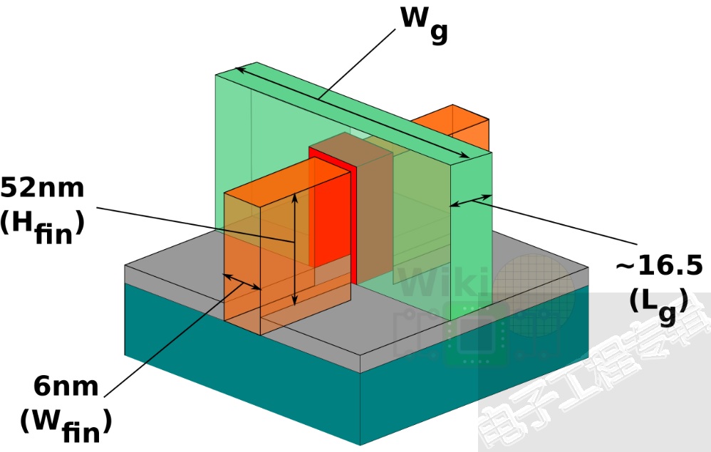
However, in fact, TSMC’s N7 process has two cell solutions, which correspond to low power consumption high density (HD) and high performance (HP). These mentioned above refer to the N7 HD low power solution. For these two different cell solutions, the fin pitch is 30nm, but the former is 57nm and the latter is 64nm.
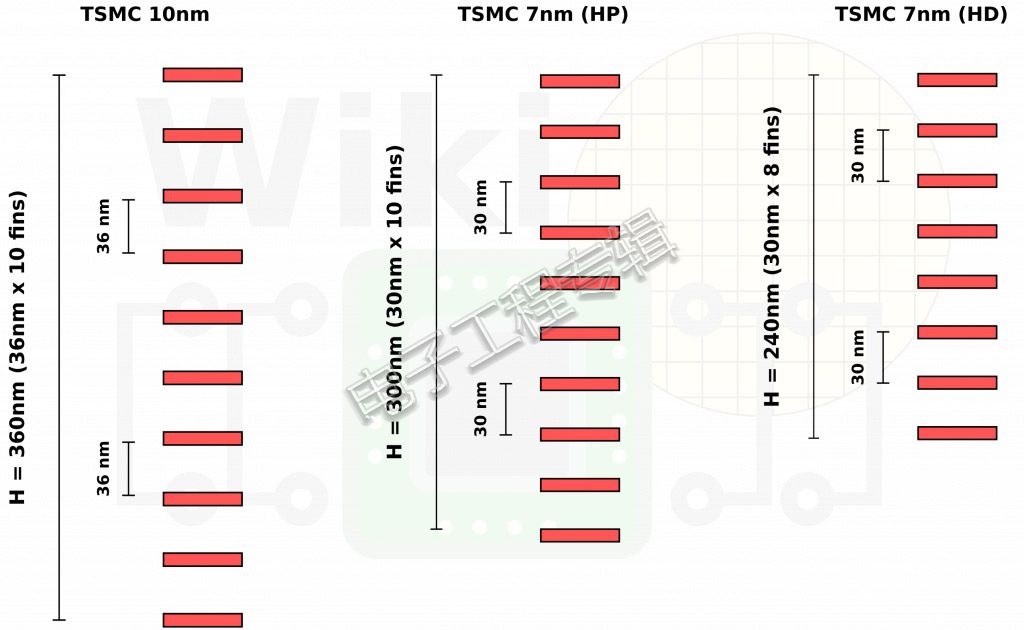
In terms of standard cells, the cell height of these two solutions is 240nm (6 track, or more commonly 6T — track refers to the track of the line; the signal line must usually go on the track, how many tracks can the standard cell height be used to represent ; 6T means that 6 lines must be walked in the range of cell height) and 300nm (7.5T). HP is 10 fin and HD is 8 fin. HP high-performance cells can achieve a higher effective drive current (Ieff) of 10-13%, at the cost of a slightly higher leakage current.
Recommended
同样是台积电7nm,苹果和华为的7nm其实不一样
Obviously, the transistor densities of the two schemes are also different. HD low-power N7 has a transistor density of 91.2 MTr / mm² (MTr refers to one million transistors, which means one million transistors per square millimeter); HP’s high-performance N7 process has a transistor density of 65 MTr / mm². What is the magnitude of these two numbers? This will be mentioned in the comparison later.
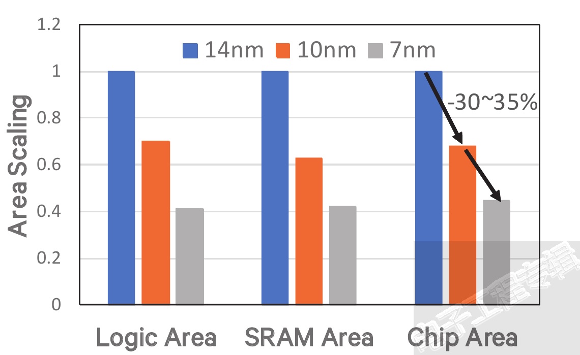
If you have no idea about these values, you can roughly understand their value by mapping them to a specific IP or product. Qualcomm said at the 2019 VLSI Symposium that the N7 process allowed Qualcomm’s Snapdragon 855 to receive a 30-35% chip area bonus (the previous generation Snapdragon 845 used Samsung’s 10nm process), including logic circuits, SRAM area and integrated chip area. Qualcomm compares the speed and power consumption curves of TSMC 7nm and Samsung 10nm processes under the typical speed path of Snapdragon 855. Under the same power consumption, the speed is increased by 10%; at the same speed, the power consumption is reduced by 35%.
Snapdragon 855 has a total of 6.7 billion transistors; its CPU is divided into three groups, one A76 core (Kryo 485 Gold) clocked at 2.84 GHz, three A76 core clocked at 2.42 GHz as a group, four clocked at 1.80 GHz A55 core (Kryo 485 Silver). Qualcomm said that the core of the 2.42 GHz group has improved performance by 20% compared to the Snapdragon 845 under the same power consumption; the small core has increased by more than 30%. Of course, this is not the dividend brought by all processes. The IP architecture design change is also relevant. Qualcomm sees the two separate factors equally contributed to the improvement.
What is more interesting is that the Snapdragon 855 uses TSMC’s two N7 solutions in the CPU manufacturing scheme: one of the high-frequency main cores uses the HP high-performance cell solution, while the other two cores use the HD low-power cell solution. It seems to be a relatively luxurious combination method, applying two methods of one process on one SoC. So even with the same N7 process, there are still differences in the same generation.
Improvement and evolution: N7P and N7+
N7 is the first generation of TSMC’s 7nm solution. Last year TSMC introduced N7P (N7 Performance-enhanced version), or the second generation 7nm. This is an improved version of the N7’s original solution. It still uses DUV and the same design guidelines, and is fully IP compatible with N7.
N7P has an optimized front-end-of-line (FEOL) process and a middle-end-of-line (MOL) process to improve performance by 7% under the same power consumption conditions, and to reduce power consumption by 10% at the same speed.
The Apple A13 SoC of the iPhone 11 series adopts the N7P solution, and the Snapdragon 865, which will be mass-produced this year also uses this process. It seems that many people are puzzled that the Snapdragon 865 does not use EUV.
N7+ and N7P are different. The former has begun to rely on EUV (extreme ultraviolet) lithography in some key layers. Its mass production began in the second quarter of 2019. N7+ has a 1.2 times density increase according to TSMC (the density here should be referred to as the transistor density), thus improving performance by 10% at the same power consumption and reducing power consumption by 15% at the same performance. In short, N7+ will be better than N7P. When it announced N7+, TSMC said that the N7+ process manufacturing yield was basically the same as N7.
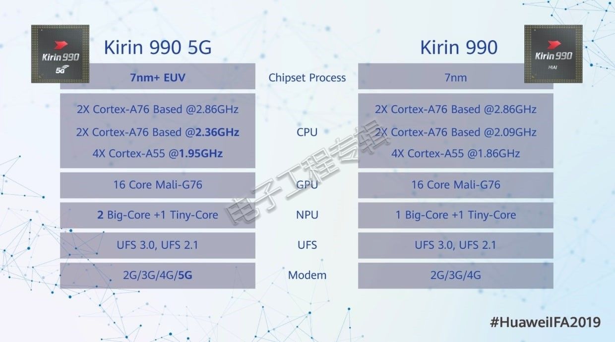
Hisilicon’s Kirin 990 5G version is built using the N7+ process. It is therefore not only a replacement of Hisilicon’s preceding Kirin modem module (built to work with 4G networks), but also a renovation of the process and some physical layers. When the Kirin 990 series was released, Huawei declared that the Kirin 990 5G was “the first chip built using the EUV process” in the industry. The Kirin 990 5G does boost the frequency of CPU and GPU to a certain extent. Its “big core” of NPU adds one more core. Unfortunately, there is no technical analysis firms who give the die in and chip area data of the Kirin 990 4G version, so it is impossible to compare the improvement of N7 + over N7 in area efficiency.
It is worth mentioning that the N7+ EUV lithography layer is 4 layers. According to news reports last year, TSMC has further introduced N6 (6nm) process nodes and will use more EUV layers (at least 5 layers). N6, however, is not a long-term node. N6 is compatible with N7 in terms of design guidelines and IP. In other words, the chip design can reuse the same design ecology of N7, such as the same tools, to directly reduce development costs. The design of N7 can be taped again on the N6 node, and it has also improved in the EUV mask and fidelity improvement; poly over diffusion edge (PODE) and continuous diffusion (CNOD) standard cells can achieve a density increase of 18%.
N6 and N7+ seem to be two different paths, because N7+ is incompatible with N6 — and N+ actually has a slight advantage in density. This may also be the reason why the Snapdragon 865 did not choose N7+ this year, and the transition of N7P and future architecture design may be smoother. During the earnings call in May last year, TSMC stated that most N7 customers (not N7+ customers) will eventually switch to the N6 process. TSMC is expected to complete the risk production of N6 earlier this year, and by the end of this year, the yield and output will be improved. This node will be carried out at the same time as N5.

Subscribe to Newsletter

Test Qr code text s ss
