HoloLens 2, Neural Probes and More at Imec’s Summit
Article By : Rick Merritt

Speakers described work on everything from mixed-reality to deep learning, solid-state batteries and brain science at Imec's annual event
Once a year the Imec research lab opens the doors to its diverse labs and invites guests for a tech show and tell. A sampler below from this year’s event, renamed Future Summits, includes a look inside the new Microsoft HoloLens and a novel quantum computer, an update on brain science and more.
You never know who you may bump into in the halls of this event. I turned around at a coffee stand and saw Jelle De Smet (below), an optics researcher I first met here in 2013.
At that time he was a PhD student with ideas for an active optical lens. Two years later, he was well along on an Imec research project that aimed to pair a flexible lens with a distance sensor to determine when and how to tune the optics.
This year de Smet was three years into a startup, Morrow Optics, using a version of his liquid crystal lens embedded in sunglasses. Push a button and the “lens-in-foil” embedded in a traditional lens morphs into a standard 1x reading lens.
The product is going through user tests now with hopes to hit retail shelves befre long. A 2x version of the active lens is in develpment. On the way to the market the complex electronics he once envisioned for an iris replacement have been simplified to a battery and controller chip in the arm of the glasses.

A fresh look inside the Microsoft HoloLens 2.0
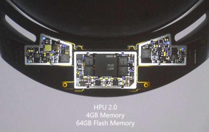
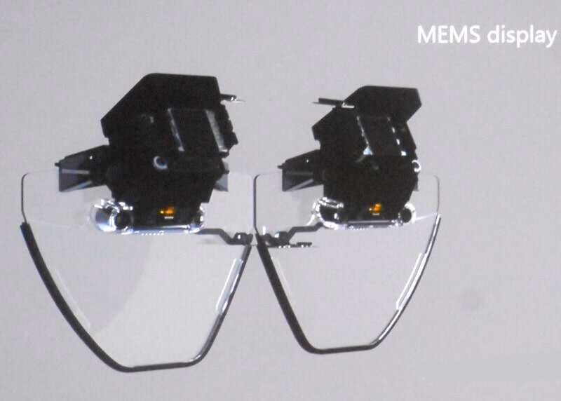
The head of the hardware team for Micrsoft’s HoloLens gave a virtual teardown of the second-generation mixed-reality headset. It sports five new ASICs, three of them controllers for a new MEMS display (bottom photo) replacing an earlier LCOS device.
The headset’s upgraded hologram processor (top photo) delivers twice the field-of-view as the first-generation and twice the pixels without twice the silicon. The resolution is crisp enough to read eight-point text, “something you better be able to do if you are from the company that makes Office,” quipped Ilan Spillinger, head of HoloLens hardware, in a keynote.
A redesigned depth sensor chip uses a 1,024 x 1,024 matrix of 3.5-micron pixels to track hand movements or map a room. The device also sports four new light sensors, upgraded cameras and a Qualcomm Snapdragon 850.
Since the HoloLens debuted three years ago as a device for developers, it has gotten market traction. U.S. regulators approved it for use in surgery and the U.S. Army agreed to buy 100,000 units for nearly half a billion dollars.
A new SEAT for top-down system-in-chip design
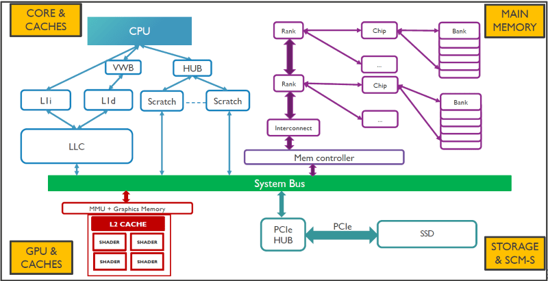
Arnaud Furnemont, a director of Imec’s memory program, provided an example of top-down design for the era of systems and silicon co-design. Imec’s SEAT (below) aims to help find system bottlenecks and test how well new technologies bust through them before designers start work on chips. [The company did not say what SEAT stands for. – ed.]
Users plug in specs, compact models and parameters and the system spits out analysis of simulated performance. It’s a direction major EDA companies such as Cadence are already validating in products.
Dense neural probes aim to map brain activity
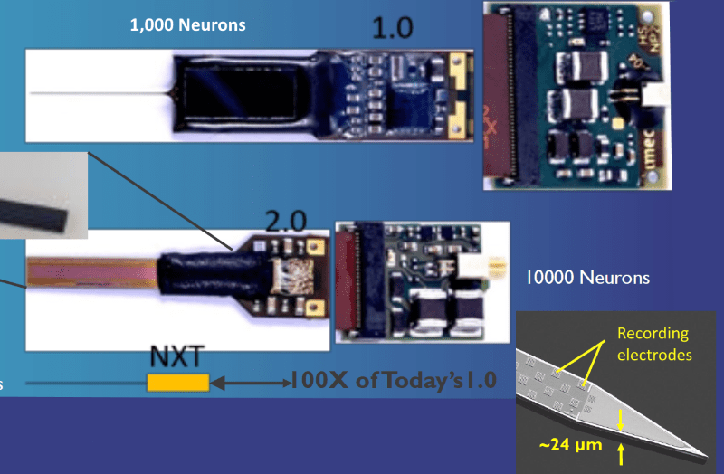
Researchers at Imec and two other insitutues designed a neural probe with a thousand active sites as part of a $10 million program. Earlier this year, they reported using several of them to simultaneously measure 30,000 neurons across 42 brain regions.
“We got a landslide of data — it was like giving someone a new telescope,” said Barun Dutta, a chief scientist at Imec who co-leads the neuropixels program.
It’s a landmark result, but still far from a long-term goal of gathering enough data to support therapies and ultimately map neural activity across the brain. Toward those goals, researchers laid out a roadmap (below) to create probes 100 times more dense by 2025.
The neuropixel packs biocompatible electrodes, made in a silicon fab, that detect ion charges. They send data at 160 Mbps across 350 channels to electronics on their shank. Researchers have already prototyped versions with integrated optical components for faster links.
Ultra-sensitive radar chips recognize gestures
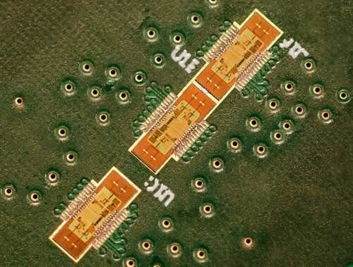
Imec designed 140 GHz radar chips so accurate they could be used to monitor the pulse of someone driving a car. The 1×4 MIMO design sports integrated antennas and has a 10GHz bandwidth, enabling it to resolve 15mm features over a 10m range.
The chips are expected to consume half the power of today’s infrared motion detectors while offering much higher resolution and similar cost. Google has reported work on a similar project at 60 GHz, but it offers half the resolution and requires external antennas.
Researchers foresee a range of uses of the three small 28nm devices (below) including gesture recognition in laptops and smartphones. The chips accurately responded 94% of the time to seven gestures using neural network models based on data from a group of 25 users.
A next-generation design is in the works supporting 4×4 MIMO using separate receive and transmit devices. The design could open the door to larger chip arrays.
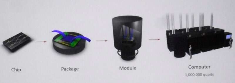
Startup rides photons in race to quantum computing
Jeremy O'Brien described the novel approach to quantum computing his startup is pursuing. He claims PsiQuantum has solved the problem of getting two qubits to entangle using light encoding with photons.
By contrast, most other researchers are working with electronic processes where qubit entanglement is not a challenge. However, they face multiple steeper hurdles correcting qubit errors and delivering systems with high speed and low cost, O'Brien said.
The startup’s system is based on a novel packaging of existing 25x25mm silicon photonics components. The modules are packed into what looks like standard 19-inch rack servers (below) that will someday sport a million qubits, he claimed.
“We are trying to make a scalable process quantum instead of making a quantum process scalable,” he said, adding his business plan includes selling quantum-computing services.
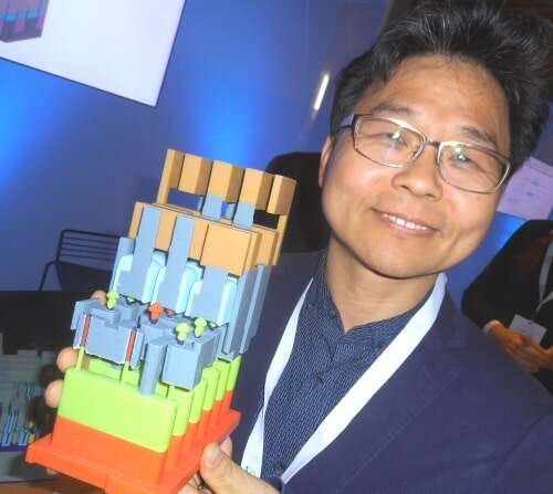
SRAM prototype based on gate-all-around transistors
Min-Soo Kim (below), a principal member of technical staff at Imec, shows a model of the gate-all-around SRAM he is designing. First silicon of a 5nm prototype looks promising, but it still needs to be optimized for the asymmetric nature of transistors that use stacked n and p elements. If all goes well, it could be one-third the size and half the power of today’s FinFET SRAMs.
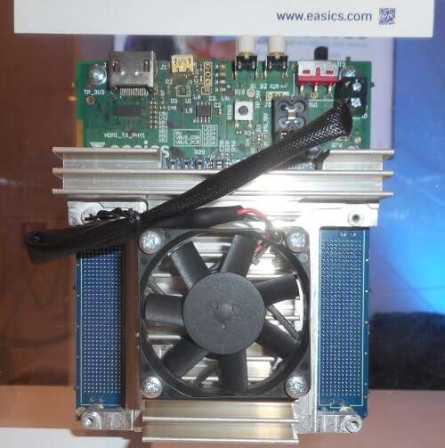
Deep learning drives image recognition system
Easics, a 1991 spinoff from Imec, demoed a deep learning system for image recognition using a convolutional neural network running on an Intel Aria 10 FPGA (below). At about the size of half a brick, the form factor of the design was a bit large for its target of IoT end nodes and it required a fan, but Easics did show it running from a battery. The company plans to work on designs using a variety of other sensors.
Chip powers patch to track second-trimester babies
Imec showed a prototype chip for a wearable patch to track a baby’s mobility and heartbeat starting as early as its 20th week of development. Previous wearables could only pick up fetal heart rate signals starting in the 30th week of pregnancy.
The BeatleIC is a five-channel electrocardiogram that operates at amplitude levels between 3- and 15μV peak-to-peak. It’s custom amplifier sports low-noise electronics and a large dynamic range to separate maternal from fetal heart beats. Power consumption is low enough to support operating a week on a coin-cell battery.
The 55nm, 2.5×2.3mm chip was designed for Bloomlife, an Imec spinoff that currently ships a patch to distinguish false from real contractions. “They were focused on the third trimester, but for their next product Bloomlife wants to go earlier in pregnancy and provide more data,” said Nick Van Helleputte, an Imec R&D manager in wearables.
Bloomlife is developing analytics based on the chip to report maternal and fetal heart rate, fetal position and other details over a smartphone app. It will start clinical trials with the device soon with plans for both a consumer product and a version for medical professionals to use as a risk management platform.

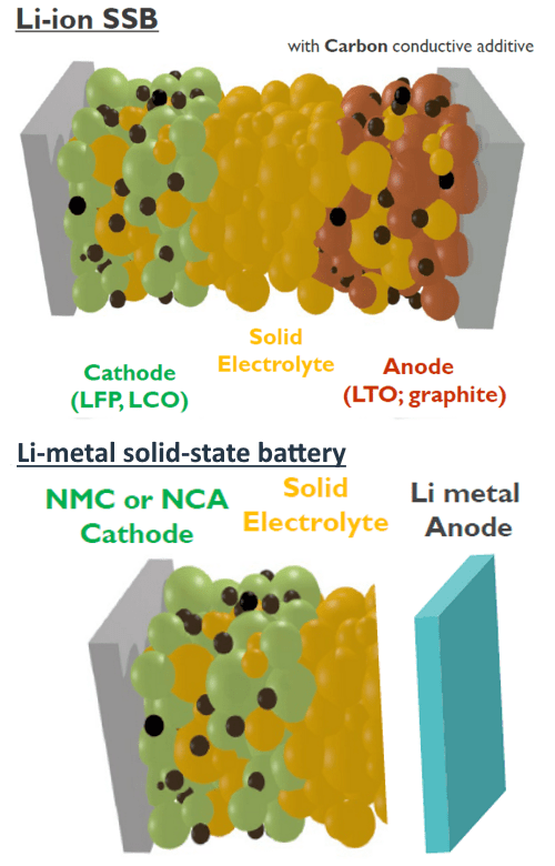
Solid-state batteries power hopes for future systems
An Imec researcher described its work on solid-state batteries. His team aims to bust through an energy-density wall that today’s lithium-ion batteries are expected to hit at 800 Watt-hour/liter by 2025.
The ultimate goal (below) is a battery using a lithium-metal anode that enables a thinner electrolyte. It also requires use of new materials for higher voltage and capacity cathodes.
If all goes well, such designs are expected to produce 1,200 Wh/l batteries by about 2030. That could enable electric cars with a range of more than 800km and smartphones that run for days on a charge.
So far, lab prototypes of solid-state batteries still lag today’s commercial products in performance. However, Imec announced a new nanowire mesh material for electrodes earlier this year and it is ramping a lab that will start producing solid-state batteries later this year.
While slow moving compared to silicon, advances in batteries have been fundamental to the evolution of electronics. They enabled today’s smartphones and electric cars and prevented wearables such as Google Glass from being successful, said Philippe Vereecken, a scientific director for battery technology at Imec.

Subscribe to Newsletter

Test Qr code text s ss
