HBM Thrives, HMC Hangs On
Article By : Gary Hilson
While high bandwidth memory (HBM) is flourishing, hybrid memory cube (HMC) is finding life in applications that didn't exist when it was first conceived.
At first glance, the rivalry between hybrid memory cube (HMC) and high bandwidth memory (HBM) mirrors the battle between Beta and VHS. But there’s one clear difference: HMC isn’t dead.
HMC uses a vertical conduit called through-silicon via (TSV) that electrically connects a stack of individual chips to combine high-performance logic with DRAM die so that memory modules are structured like a cube instead of being placed flat on a motherboard. This architecture enables much higher performance than DDR technology with lower power consumption.
The technology development was being led by the Hybrid Memory Cube Consortium (HMCC) and included major memory makers, such as Micron, SK Hynix, and Samsung, as well as other developer members, such as Altera, Arm, IBM, Microsoft, Open-Silicon, and Xilinx. But although some vendors incorporated HMC technology into their products and architectures, such as Intel, Altera, and Xilinx, it has not really taken off in the same way that HBM has, and the HMC specification never did follow through with a version 3.0. It has been adopted for some advanced, high performance computing and data science applications, too, including the Square Kilometer Array (SKA) program and in HPC solutions from companies such as Fujitsu.
Micron, which was one of the earliest and strongest proponents of the technology, does sell HMC 2.0 on FPGA modules today, said Steve Pawlowski, vice president of Advanced Computing Solutions at Micron, but rather is sticking strictly with the HMC protocol per se — the focus is on how the architecture might make sense to meet the high bandwidth memory demands of specific use cases including artificial intelligence (AI), which didn’t really exist when HMC was first conceived. “Where can we get the biggest bang for the buck in terms of very high bandwidth in low power [while] being able to get a more cost-effective packaging solution to our customers?”
Pawlowski said Micron continues to explore HMC’s potential through “pathfinding programs” rather than follow through with the original plans for a specification update, while also advancing other high bandwidth memory technologies — including the expansion for GDDR beyond the traditional graphics market and for extreme performance applications, as well as the HBM technology that came after HMC and eclipsed it.
Pawlowski said HMC was a great solution from a performance perspective, but customers were also looking for more capacity. “The bandwidth capacity trade-off was kind of skewing a little more towards the capacity.”
Emerging AI workloads, however, are more focused on bandwidth, so that’s where the HMC architecture has potential.
In the meantime, Micron has an active HMB program with a product that’s JEDEC-compliant. Its HBM2E portfolio is currently in the engineering sample phase and includes 8 GB and 16 GB offerings, and the company is also working to qualify its HBM2E on reference platforms.
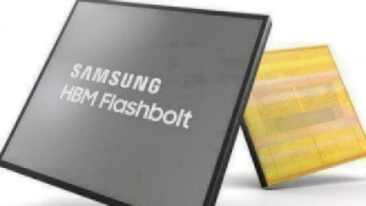
HBM has seen some consistent, incremental updates over the past few years thanks to companies such as Samsung, which recently announced its third generation, 16 GB HBM2E dubbed “Flashbolt.” It doubles the capacity of its “Aquabolt” predecessor by vertically stacking eight layers of 10 nm-class (1y) 16Gb DRAM dies on top of a buffer chip in an HBM2E package that’s interconnected in an arrangement of more than 40,000 TSV microbumps, while delivering data transfer speeds of 3.2 Gbps and memory bandwidth of 410 Gbps per stack.
Tien Shiah, senior manager of high-speed memory marketing for Samsung Semiconductor, said the HBM2E is well suited for HPC and state-of-the-art graphics systems, as well as AI-driven data analytics. “It’s clear that HBM has become a memory of choice for AI.” He said this is due in part to the fact that HBM is an industry standard, whereas HMC isn’t, and it requires IP partners to develop the ecosystem. A key technical difference is that HMC uses a serial interface, while HBM employs a parallel interface, even though both use TSV.
Because HMC wasn’t an open standard, the potential was for there to be different, propriety flavors of the technology. HBM is an open standard, so anyone can dive in create a product, said Jim Handy, principal analyst with Objective Analysis, and it’s now finding itself in demand by hyperscalers and for AI applications, not just the initial HPC and high-end graphics systems. “What HBM brings to the party is a screaming fast interface way faster than DDR.”
What makes both HMC and HBM premium memory is the use of TSVs, which dramatically raises the manufacturing costs. Even though AI and hyperscalers have opened the floodgates for HBM demand, said Handy, relatively speaking it’s still manufactured in low volumes. “It’s not something that you would expect to become really widespread because it still is a very premium priced kind of a solution.”
Shiah also said HBM will always be a premium type of memory because it’s more costly to manufacture. “But with more volume and applications adopting it, I think you’ll see the economies of scale.”
Samsung has steadily and incrementally improved its HBM offering since introducing its Flarebolt iteration in 2016, followed by its second generation HBM2, Aquabolt, in 2018. “If you look at our latest offering HBM2E, it basically increased the speed by up to 75 percent and doubles the capacity compared to our previous generation,” said Shiah. Ultimately, HBM is the fastest form of DRAM available, which appeals to customers looking for the fastest solution available for AI and machine learning applications. It’s also being looked at for autonomous driving applications to support the instantaneous decision making required.
While there are many emerging memories out there being explored for new use cases, nothing’s faster than DRAM, even 3D Xpoint, which is now available as Intel Optane DIMMs, which is how DRAM is typically used. “Certainly, the bandwidth throughput of HBM is unrivaled,” said Shiah.
In the meantime, it looks as though HMC is still alive and that its architecture might make sense for applications that didn’t really exist when it was first conceived. Pawlowski said HMC is an excellent example of technology that was ahead of its time and needed to build an ecosystem for it to become widely adopted. “My gut is an HMC-style architecture kind of falls in that camp.”

Subscribe to Newsletter

Test Qr code text s ss
