Extending Moore’s Law using oxygen layers in CMOS
Article By : R. Colin Johnson
The Mears Silicon Technology can be applied at any node—from legacy 180nm nodes to mainstream 28nm nodes to the most advanced 10-to-7nm nodes.
Robert Mears, the man who invented the Erbium Doped Fibre Amplifier (EDFA), believes Moore's Law could be extended again—sans scaling.
EDFA is the first commercial and still popular method of amplifying optical signals without having to convert them into electrical signals (and back again). Now, Mears said he has invented an equally industry-changing technology for CMOS called the Mears Silicon Technology (MST) at Atomera Inc.
"At Atomera our vision was how to structure silicon so it had electrical properties that would allow it to work with other types of materials. It was created in computer simulations, then realised on wafers," Mears told EE Times. "Our whole purpose at first was to boost electron- and hole-mobility simultaneously, but then we discovered all these other advantages that went along with it."
![[Atomera Moore transistor 01 (cr)]](/wp-content/uploads/sites/2/2020/04/Atomera_Moore_transistor_01_cr.jpg)
__Figure 1:__ *A cross-section image of the Mears Silicon Technology (MST) where oxygen superlattice layers in the channel of a transistor (red) increase mobility and drive current while lowering leakage. (Source: Atomera)*
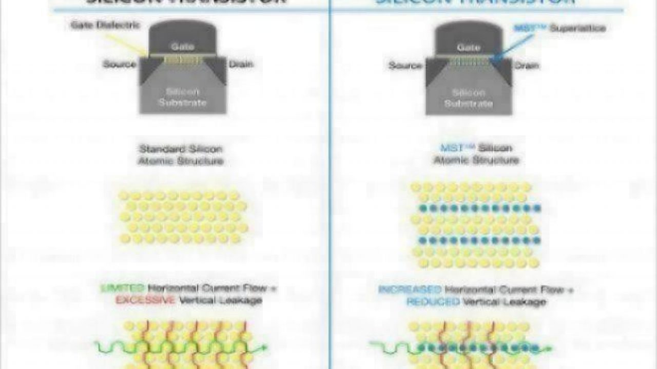
MST epitaxy inserts oxygen sub-monolayers between the transistor channel's crystalline lattice layers as they grow (see figure). Mears claims that the result not only enhances carrier mobility, but also provided higher drive current and lower leakage current (by as much as 50%). The oxygen does not bond with the channel material making an insulating oxide, but rather acts as a superlattice that invokes quantum confinement principles to enhance performance. The performance improvements can also be traded-off for smaller chip area (at the same performance) but lower cost, as well as reduced supply voltage for a power reduction (at the same performance).
"The MST process is an epitaxial grown silicon step put down during silicon deposition using standard equipment," Mears said. "During growth we stop at periodic interval and put down a monolayer of oxygen creating a very subtle disturbance in the silicon lattice for conditional confinement that squeezes that conduction region ending up reducing the scattering of electron and holes."
![[Atomera Moore transistor 02 (cr)]](/wp-content/uploads/sites/2/2020/04/Atomera_Moore_transistor_02_cr.jpg)
__Figure 2:__ *Atomera’s MST quantum confinement superlattice layers (right) compared to a normal CMOS transistor (left). (Source: Atomera)*
Claimed performance enhancements that Mears' team discovered also include improved reliability and reduced variability (for higher yields and better transistor matching, respectively) due to a "more ordered, steeper retrograde well/channel profile for better channel doping."
The amount of performance enhancement depends on many factors, according to CEO, President and Board Director Scott Bibaud, but "ranges between 10-and-25%." The good news is that MST can be applied at any node—from legacy 180nm nodes to mainstream 28nm nodes to the most advanced 10-to-7nm nodes. For instance, Atomera published a paper on next-generation SRAMs in the April 2016 issue of the IEEE Transactions on Electron Devices titled Analysis of 7/8-nm Bulk-Si FinFET Technologies for 6T-SRAM Scaling. There they stated that "using a MST punch-through stop layer facilitates reductions in SRAM minimum operating voltages by ~15% and area savings of ~20% in the SRAM cell.
"We make a technology that adds to the CMOS process mobility enhancements plus many other side benefits, including higher performance, lower power consumption, better yields and lower costs," Bibaud told EE Times. "Use our technology to increase performance by the same amount as going to the next design node—rather than continuing to shrink. With MST we believe that 28 nanometre will be the most popular node for the next decade, because only very large dies make it worth the move to 22 nanometre."
Mears invented MST just after the turn of the 21st century and has been hard at work with his team at Atomera ever since perfecting the technique and proving the concept for microprocessors, DRAMs, SRAMs, flash, other memory technologies, power-management chips, radio-frequency (RF), analog and mixed‐signal devices. The company's business plan is to license its technology—which is protected by 55 U.S. Patents and over 150 International Patents—to every major semiconductor maker. After all, all fab owners want more bang-for-their-buck and Atomera promises to deliver it.
"There are three ways MST can solve Moore's Law," Bibaud said. "For legacy nodes for analog and power devices, such as 180-, 130- and 90-nanometre, they can shrink their die size while getting the same performance. At 65-, 40- and 28-nanometre MST can give a new level of performance and lower power at the same node, allowing fabs to be productive longer. And at very advanced node like 16-, 14- and 10-nanometres, FinFETs using MST will allow fabs to continue using bulk silicon rather than going to other materials like III-V channels."
Atomera is keeping its hand close-to-its-vest on its future growth opportunities—besides saying that it hopes to work its way up from legacy silicon nodes to popular- and then advanced-nodes. However, it claims to have even higher goals in sight. For instance, Mears photonics-amplifier fame has gotten his mental gears turning on how to enhance optical and solar devices with MST. And according to Bibaud the company also has improvements of magnetic materials for next-generation advanced memories in sight.
So far, however, the company is only revealing how standard complementary metal oxide semiconductor (CMOS) fabs can easily integrate MST into the conductive channel of their transistors. One paradox, however, is that on the one hand it emphasises how easy it is to "merely" modify a fab's epitaxial layer design. On the other hand, it claims their adopters will also need consulting services to to optimize the oxygen superlattice layer for particular applications.
One thing is for sure, Atomera needs that revenue stream to get it out of the red since mass production could be years away. The company recently went public as ATMR and now has to answer to stockholders. Accordingly, it is hoping to cash in on licensing and consulting for the $350 billion semiconductor market, prompting Nasdaq to allow Bibaud to ring the exchange opening bell on August 18, 2016.
On the positive side, Atomera says their cost-per-wafer is lower than alternative CMOS enhancement techniques that extend the lifetime of a fab's infrastructure including "stress memorisation, embedded-SiGe, Dual Stress Liner, SOI [silicon on insulator] and HKMG [high-k metal gate]."
On the negative side, Atomera claims to have taken their technology to most big fabs, but have only convinced three legacy fabs to sign-on. And what is even more curious, Atomera claims to have never briefed any analysts I could interview to get an unbiased evaluation of MST.

Subscribe to Newsletter

Test Qr code text s ss
