Examining metal eFuses
Article By : Kevin Gibb

We first scrutinised the eFuses in Intel‘s 32nm high-k metal gate (HKMG) fabbed Westmere/Clarkdale processor (circa 2009). At the time, Intel was using the eFuses as part of a one-time programmable read-only memory (OTP-ROM). We now appreciate that their use can include the holding program code, on-chip configuration data and cryptographic keys. Prior to metal […]
Prior to metal gates, electrically-blown on-chip fuses were typically made from the polysilicon gate layer. But with the advent of metal gate CMOS processes, polysilicon was no longer available as a fuse element. What to do?
Intel had published a paper on their 32nm OTP-ROM (Kulkarni et al. J. Solid-State Circuits 2010) where they had used electrically blown metal fuses (eFuse) as memory elements. The fusing element is made from a via 2 that connects a metal 2 bus to a metal 3 line. Their three-dimensional heat modeling shows the upper portion of the via to be the fusible element.
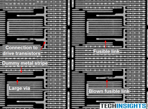
But, we find the fusible links (or fuse) in the Westmere/Clarkdale processor to be implemented as metal 1 traces as shown in figure 1.
 |
|
Figure 1: Two blown fuses and six intact fuses can be seen in this image, along with interconnects to underlying drive transistors. The blown portions of the fuses have irregular shapes that are consistent with the electromigration (EM) of the copper atoms making up the metal 1 lines. Source: Custom Analysis of the eFUSE Structures used in the Intel Westmere Clarkdale 32nm Processor, TechInsights |
Intel’s paper describes this void formation (fusing action) as being based on thermally assisted electromigration.
Large vias can be seen at the left ends of the fuses and are used to keep the current density low at the via bottoms. This ensures that the electromigration voiding will occur in the fusible link.
The mean time to failure (MTTF) for a metal wire undergoing electromigration is given by the Black’s equation (1) (JEDEC JESD63, 1998)
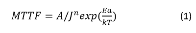 |
Where J is the current density, T is temperature, Ea is an activation energy of about 0.9 eV, A is a constant, k is Boltzman’s constant and n is a model parameter that ranges from 1 to 2. We take n= 1 in this article.
We can use equation (1) to estimate how long it will take to blow Intel’s eFuse and to do this we have measured the fuse’s cross sectional area (1×10⁻¹⁰ cm2), estimated a 12 mA constant drive current for the MOS drive transistors used to blow the fuse (~ 1.2×10⁸ A/cm2). We have some MTTF data of about 440 hours for a Damascene copper wire under a 1.5 mA/cm2 bias current at 300 oC (R. L. de Orio et al. VLSI-SoC conference 2009). This 440 hours MTTF is inferred from one of their graphs is subject to a fair bit of uncertainty.
Intel’s paper shows their fuse as having a 1,000 oC hotspot at the top of the via, but the Westmere/Clarkdale eFuse is implemented as a strip of metal 1. We doubt the metal 1 fuse self-heats to 1,000 oC but 500 oC does not seem too unreasonable. This assumption combined with equation (1) yields a MTTF of about 0.2?s. Intel has used 2 V bias pulses of about 1?s duration to blow their fuses so our 0.2?s estimate is not far off the mark.

Subscribe to Newsletter

Test Qr code text s ss
