EE Times Revives ‘Under-the-Hood’
Article By : Junko Yoshida
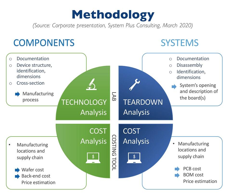
System Plus teardowns go beyond listing ICs to identifying packaging, IP blocks and even circuit construction, so that it can calculate accurate costs. The company calls it “reverse costing.”
NANTES, France — Ever since Pandora, everyone wants to know what’s inside the box. In electronics, this irrepressible curiosity applies to the newest iPhone, Android or Fitbit, or under the hood of an Audi or Tesla.
Who wouldn’t?
Pulling boxes apart has been a pastime (or passion) for most of our readers since they were toddlers. Now they’re professional engineers, and prying off the back of the gadget goes beyond mere pastime to a quest for competitive knowledge.
EE Times is happy to announce our “Under-the-Hood” series is back, this time, in partnership with System Plus Consulting.
System Plus Consulting (Nantes, France) is a part of Lyon-based boutique market/technology research firm Yole Développement. Backed by 27-years of history in cost-modeling expertise and database, System Plus isn’t standing still. Last year it acquired an Austin, Texas-based team that specializes in consumer product teardowns, previously owned by ABI Research.
Because there are many specialists and market research firms racing to track down and take apart the latest model of Samsung, Apple, HTC or Huawei devices, teardown is a fiercely competitive business. In this light, what makes the System Plus team think they’re special?
It’s not enough to know design wins
a recent interview with EE Times, Romain Fraux, System Plus CEO, speaking of teardowns, stressed “Knowing design wins isn’t enough.”
Teardown isn’t a hobby.

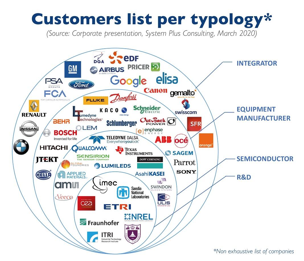
System Plus serves a broad base of clients, from researchers at R&D institutes and chip designers at semiconductor vendors to OEMs, service operators and platform giants. They all want to know not just what’s inside the box, but why certain technologies and specific components were picked, and how much it costs to manufacture such a device. Cost analysis from chips to a system, when done right, can lead System Plus analysts to deduce the next likely move for device or system vendors.
System Plus pointed out that knowing the physical and electrical characteristics of a product is critical. But “the cost of a product must be considered as a performance.” In other words, the job of negotiating a better price for components falls to purchasing managers. But for design engineers, knowing the actual cost of devices and factoring that into the initial system-definition phase can create a competitive edge.
Going beyond BOM analysis
Of course, most teardown outfits also deliver in their reports a list of chips and components designed into a system, as they offer their own analysis on the bill of materials (BOM).
System Plus, however, drills further down in its cost analysis.
Beyond delivering a report on design wins, System Plus — often in close collaboration with Yole’s analysts — offers insights on trends in technology and markets. Further, the team examines system vendors’ technology choices and shows how a company’s thinking might have evolved. The iPhone 11 Pro is a good example. System Plus focused on what Apple either dropped or added in the new smartphone handset compared to iPhone 8.
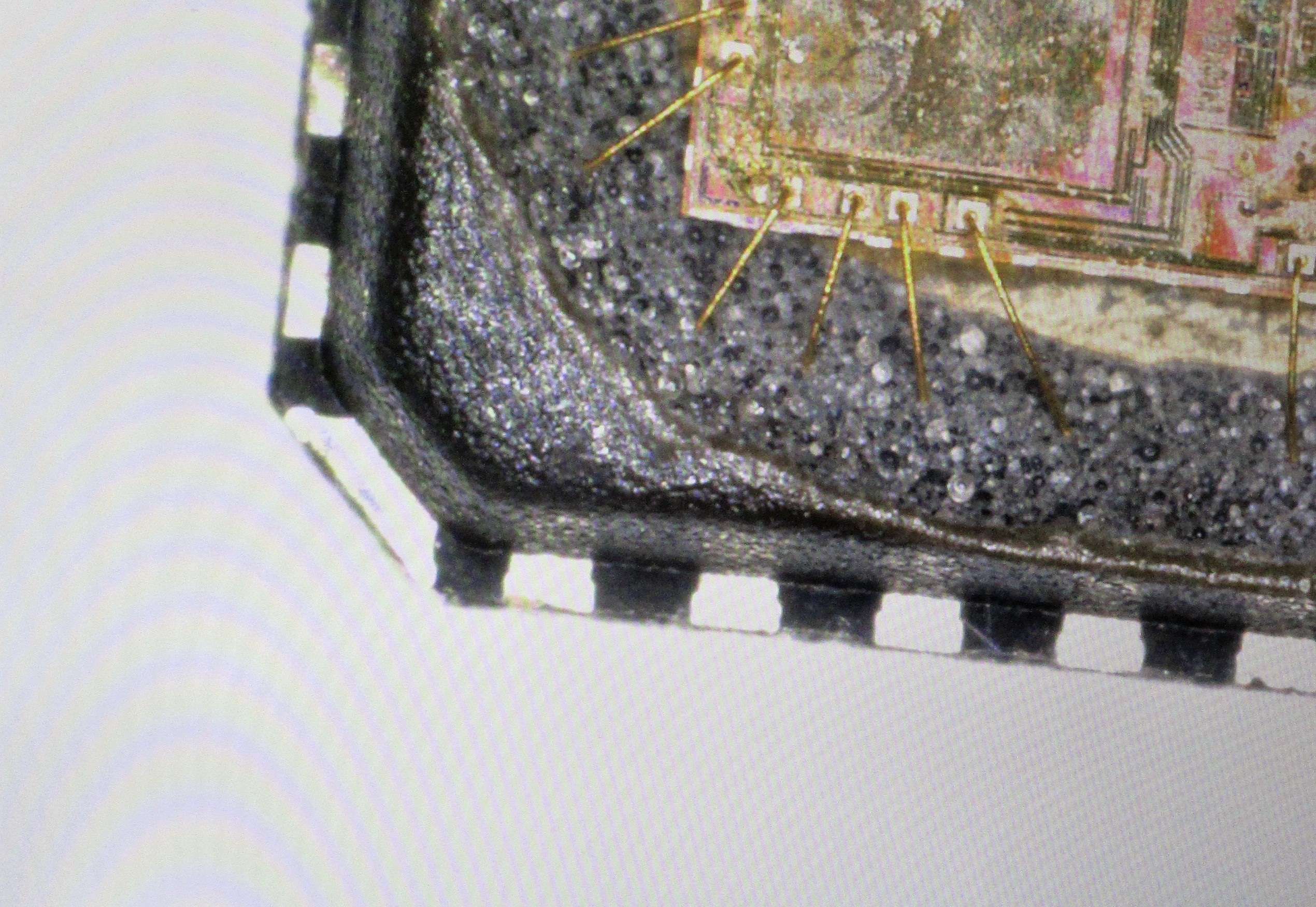
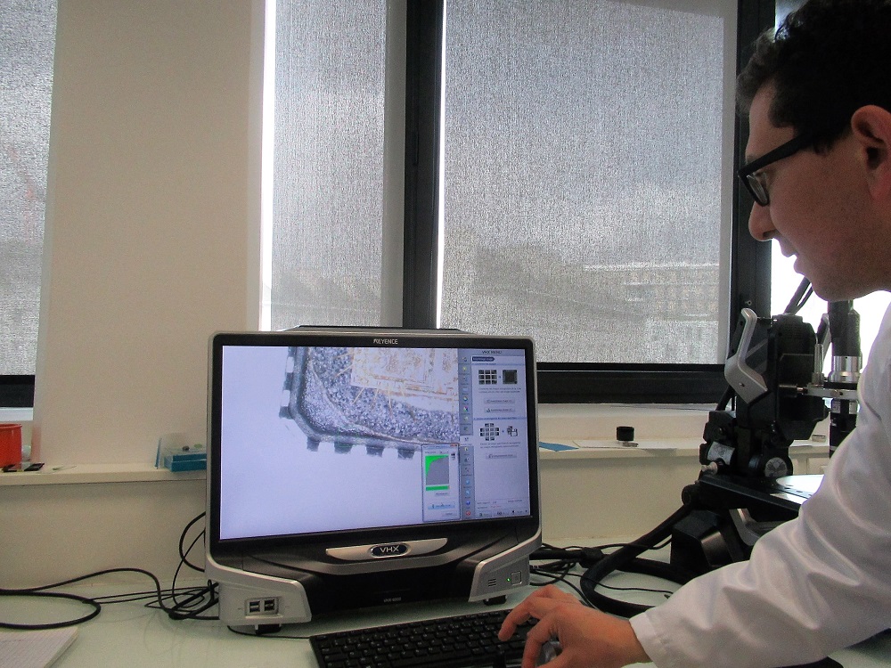
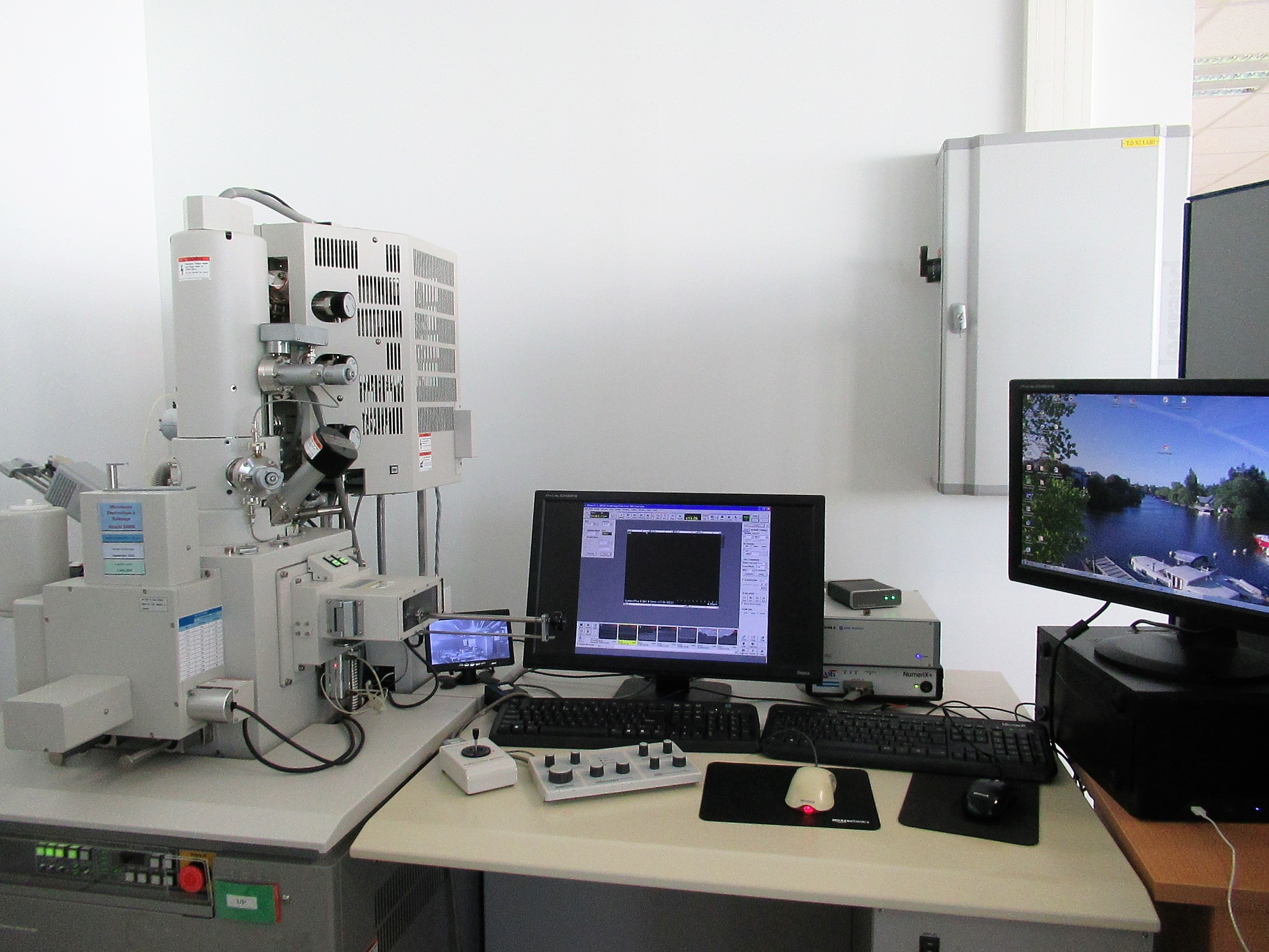
System Plus also studies die-level integration. It examines the structure of a chip and peels the chip layer by layer by using the company’s own tools so that it can identify its structure, types of materials used, and their volume of such materials applied to the device.
As System Plus looks at everything from systems, SoC and chip structures to packaging, and IP blocks designed inside an SoC, down to the different materials in a semiconductor device, Fraux explained that his team’s mission is to identify technologies and calculate manufacturing cost. The company calls this “reverse costing.”
Reverse engineering vs. reverse costing
“Reverse engineering” we know. What exactly is “reverse costing”?
Reverse engineering exposes how a system is put together by cracking open a box, examining its content and drawing up a schematic. Once these schematics become available, others can presumably copy the design and build the same system.
On the other hand, “reverse costing is the foundation of technical analysis of manufacturing cost,” according to System Plus.
Fraux explained, “At System Plus, we do not extract design from components, but we extract ‘process’ from a device. Our goal is to reconstitute manufacturing/production process, so that we can estimate approximate cost to produce these components.”
System Plus’ reverse costing takes “a bottom-up approach,” Fraux said. It does cost analysis both on the component and system levels.
On the component level, for example, the team looks at a device’s structure, identifies its ingredients, measures its dimension and examines as cross section as layers are peeled away. Such a process usually gives away knowledge of how the component was manufactured. Combined with publicly available information about manufacturing locations and supply chains, the team can estimate wafer and back-end costs so that it can derive a price estimate of the component.
Similarly, on a system-level cost analysis, the team disassembles the system, identifies components inside and measures dimensions, which results in description of board(s). Again, by leveraging public information of production locations and supply chains, the team estimates PCB and BOM cost, leading to a price estimate.
Cost estimation: ‘Not an exact science’
Nonetheless, Fraux is quick to acknowledge, “Structural Analysis is math. But cost estimation is not an exact science.” This is where the technology and business/financial analysts meet.
The team reads quarterly financial reports issued by companies backward and forward. They keep a close eye on the latest developments in the industry’s business activities, reported by financial news and reports.
As Fraux explained, the team does cost estimation often based on “our hypothesis, assumptions — coupled with our own understanding of the industry.” Since no company is inclined to disclose such proprietary information as margins and yield rates, a lot must be deduced from what System Plus and Yole know.
Acknowledging that System Plus could come up with a wrong hypothesis, Fraux said, “We’re keeping an open mind. We know that costing is not easy. So, we use our report to open the dialogue with the industry.”
While the Austin, Texas team is focused on consumer products teardowns, analysts in Nantes specialize in industrial and automotive products. “While we don’t tear down the entire car,” said Fraux, “we look inside certain ‘parts’ of a car — including ADAS, telematic, and infotainment units.”
Today, System Plus has “five teardown tracks” and “seven component streams.” Teardown tracks include:
- phones including smartphones and feature phones,
- smart home including smart speakers and home assistants,
- wearables from smart watches to earbuds,
- connected devices (110+ products) including tablets, and
- automotive including ADAS, infotainment, Telematic control units.
System Plus also offers “component streams,” including apps processors, audio and power management, baseband, connectivity, memory, RF and sensors.
Nantes, the home of System Plus Consulting, is also the birthplace of Jules Verne. Historically, the city grew up as the largest port in France for the triangular trade among France, Africa and South America for manufactured goods, slaves and sugar.
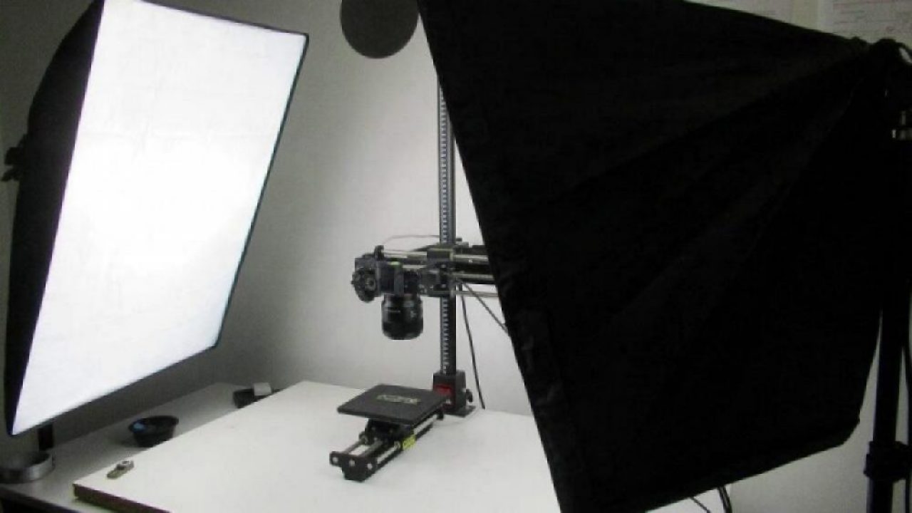
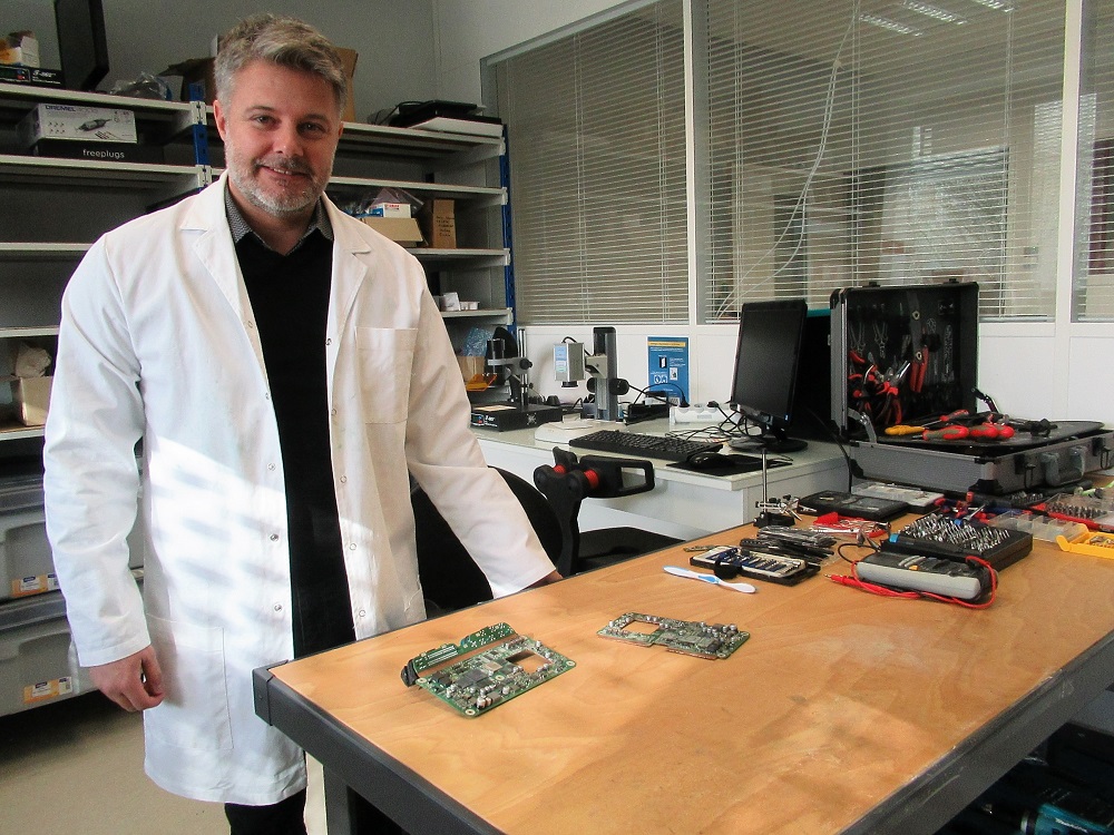
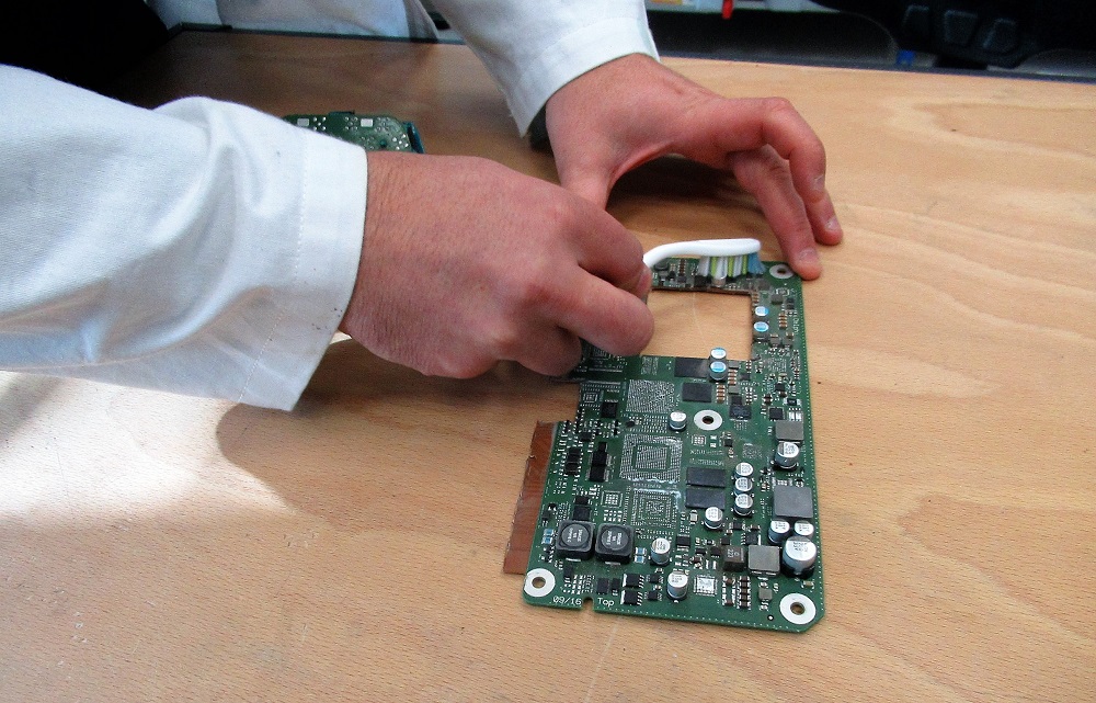
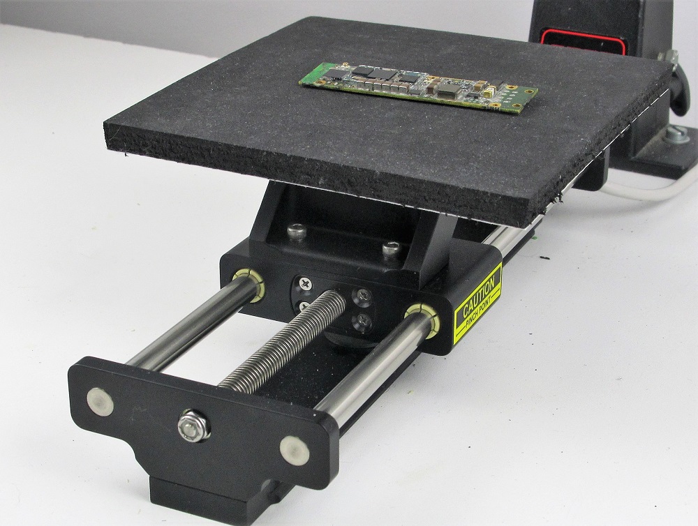
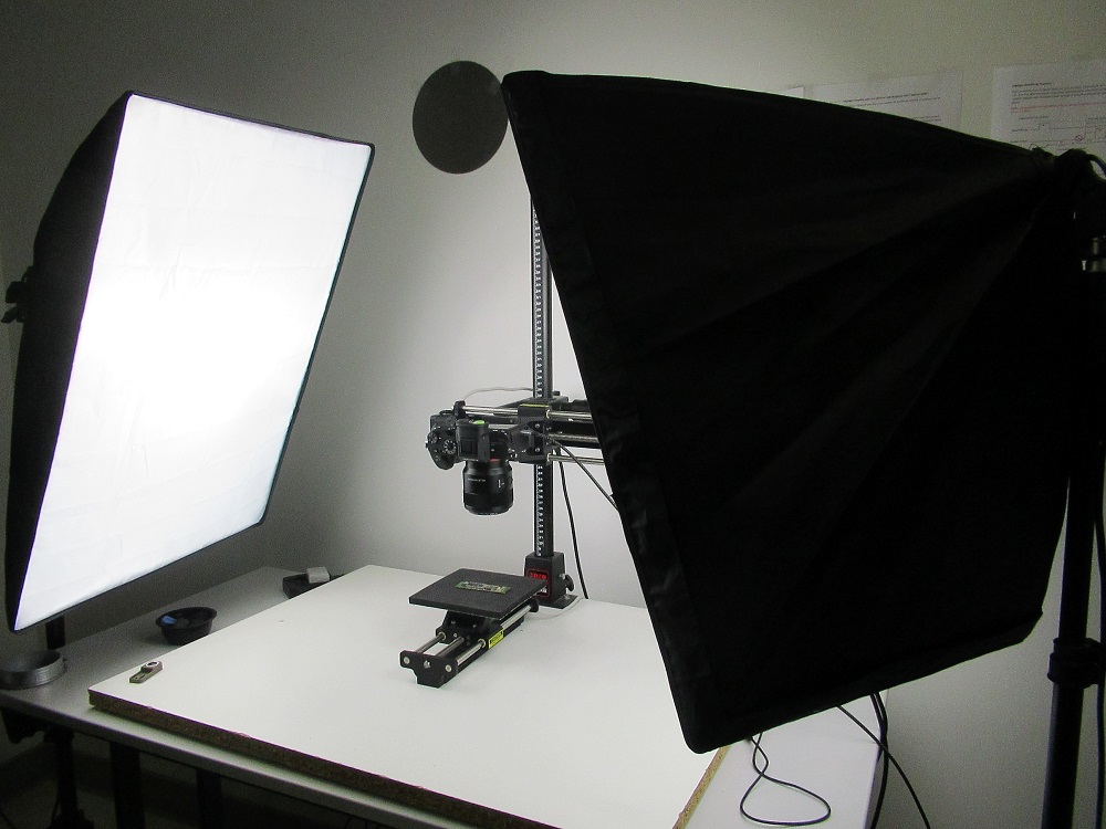
Following are a few pictures shot during EE Times’ visit to System Plus.


Subscribe to Newsletter

Test Qr code text s ss
