CMOS electronics, Si-photonics integration targets 1Tb/s
Article By : Julien Happich
The COSMICC-developed technology will address future data-transmission needs with a target cost per bit that traditional WDM transceivers cannot meet.
The COSMICC project, launched by Leti, aims to combine CMOS electronics and Si-photonics with high-throughput, fibre-attachment techniques.
These scalable solutions are expected to provide performance improvement an order of magnitude better than current VCSELs transceivers, and the COSMICC-developed technology will address future data-transmission needs with a target cost per bit that traditional wavelength-division multiplexing (WDM) transceivers cannot meet.
Currently, the project’s 11 partners from five countries are focusing on developing mid-board optical transceivers with data rates up to 2.4Tb/s with 200Gb/s per fibre using 12 fibres. The devices are expected to consume less than 2pJ/bit and cost approximately €0.2 per Gb/s.
“By enhancing an R&D photonic integration platform from project member STMicroelectronics, the partners in COSMICC aim to demonstrate the transceivers by 2019,” said project leader Ségolène Olivier of Leti. “We also plan to establish a new value chain that will facilitate rapid adoption of the technologies developed by our members.”
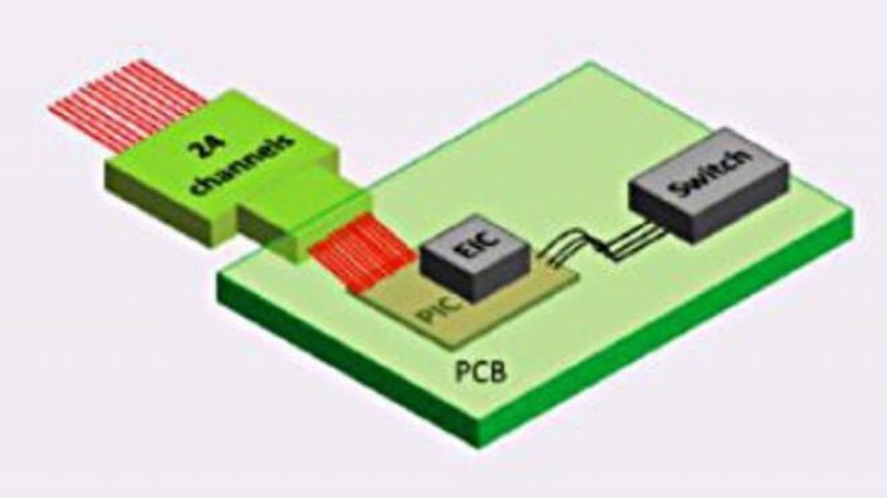
![[Leti COSMICC 01 (cr)]](/wp-content/uploads/sites/2/2020/04/Leti_COSMICC_01_cr.jpg)
__Figure 1:__ *Schematic of COSMICC on-board optical transceiver at 2.4Tb/s (50Gbps/wavelength, 4 CWDM wavelengths per fibre, 12 fibres for transmission, 12 fibres for reception.*
Several technological developments will be used to boost the photonic integration platform’s high data-rate performance, while also reducing power consumption. A first improvement will be the introduction of a SiN layer that will allow development of temperature-insensitive MUX/DEMUX devices for coarse WDM operation. In addition, the SiN layer will serve as an intermediate wave-guiding layer for optical input/output to and from the photonic chip.
Additional steps will enhance modulator performance to 50Gb/s, while making the transceivers more compact and reducing energy consumption. The partners will also evaluate capacitive modulators, slow-wave depletion modulators with 1D periodicity and more advanced approaches. These include GeSi electro-absorption modulators with tunable Si composition and photonic crystal electro-refraction modulators to make micrometre-scale devices. In addition, a hybrid III-V on Si laser will be integrated in the SOI/SiN platform in the more advanced transmitter circuits. Project demonstrators will be tested in both lab and field environments.
In addition to project coordinator Leti, other participants include STMicroelectronics (France), STMicroelectronics (Italy), University Pavia (Italy), Finisar (Germany), Vario-Optics (Switzerland), Seagate (UK), University Paris-Sud (France), University St. Andrews (UK), University Southampton (UK) and Ayming (France).

Subscribe to Newsletter

Test Qr code text s ss
