Chip Performance may no Longer Scale
Article By : Rick Merritt

Semiconductor gate and pitch dimensions are slowing to a stop, but researchers see ways to drive advances down to the 1-2nm node
The next-generation transistor may come in Intel, Samsung and TSMC flavors. It’s just one sign of how the semiconductor roadmap is fanning out as it approaches a frightening wall a few nodes ahead.
At an annual event in Belgium, Imec researchers laid out what one observer called “a Cambrian explosion” of options to squeeze advances out of silicon. They span new kinds of transistors, materials, architectures and packages.
“Generic devices may no longer be possible…the one-dimensional roadmap may not be sufficient anymore. The future is not clear, but we need more options,” Luc van den Hove, chief executive of the research institute, said in a keynote.
Engineers will need all the knobs and levers they can get given a sobering roadmap Imec showed. It forecasts feature sizes will plod forward with shrinks at a pace measured in single-digit nanometers for the next few nodes. Beyond 40nm gate lengths and 16nm metal pitches at a 2-nm node, they may not shrink at all.
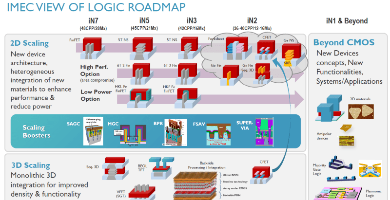
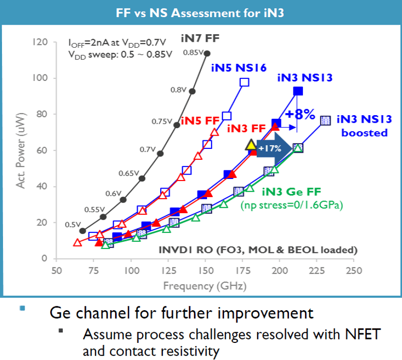
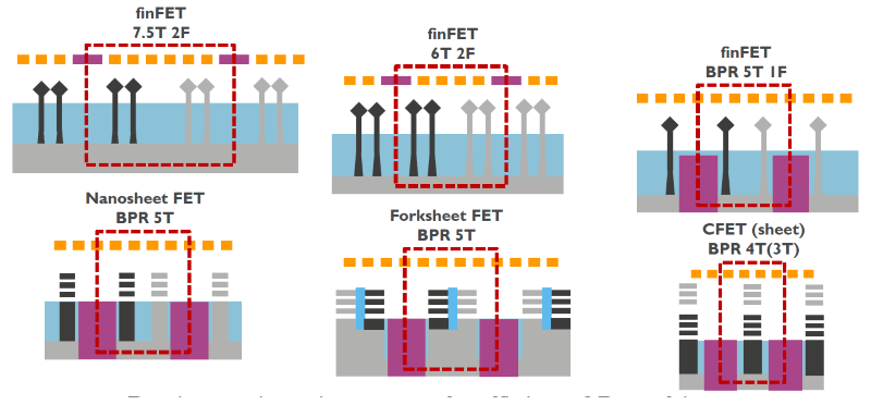
The result is chip performance may no longer scale for the highest-end parts. Shy of the top-end in active power, advances still are possible, especially for those willing to switch from FinFETs to more compact nanosheet transistors.
Chip makers focused on area and power shrinks for mobile systems may cling to FinFETs as long as possible. Those most hungry for performance gains will shift early to nanosheets that Imec expects will eke out an extra 8% in frequency, sacrificing reductions in area.
Nanosheets will have an emerging mid-life kicker in what Imec calls the forksheet, a design still being defined that pushes n- and p- devices closer together. The ultimate in compact transistors is a complementary or vertical FET that could get down to four or even three tracks by stacking n and p elements.
Along the way, engineers may try to push spacers to k values as low as 3.3 or even make a mad leap to germanium structures. “It’s a lot of each going their own way,” said Julien Ryckaert, director of Imec’s logic scaling program.
Designers working at standard cells and higher levels can ignore the transistor variations but will face extra cross-checks if they want to change foundries. Fabless companies with their own memory macros and cell libraries will need to be “profoundly aware of what’s happening on the technology side,” said Diederik Verkest, an Imec program director.
Reworking SoCs, liquid cooling chip stacks
A handful of emerging wafer, chip and transistor stacks will provide additional traction, essentially disintegrating the traditional SoC. However, the techniques present their own challenges in device alignment and cooling for designs expected to push thermals beyond 500W.
Imec described a radical reworking of the SoC it calls sequential 3D that separates and optimizes for the different needs of power, logic and memory circuits. One version puts power delivery circuits on the backside of a wafer thinned to a few hundred nanometers and connected with tiny though-silicon vias.
A more ambitious version puts SRAM cache on a carrier wafer above the core using copper-to-copper bonding. The ultimate in sequential 3D is a sandwich with the SRAM array at the bottom, power circuits at the top and core logic in between, maximizing SRAM size while lowering costs.
The approach opens a door to integrating various kinds of devices such as passives. However, an initial 5nm demo Imec built did not include any active structures.
“It’s a new playground…There’s a whole roadmap possible here so Moore’s law isn’t dead,” said Ryckaert.
Somewhere on the journey to a 1-2-nm node, engineers will need to swap out copper and cobalt, probably for ruthenium. The material lets designers thin barriers currently used to prevent today’s metals from diffusing into silicon dioxide layers.
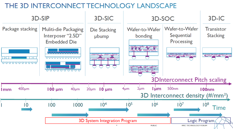
Beyond the die, researchers discussed a half dozen other packaging techniques. For example, Imec is working on a cheaper variant of Intel’s EMIB that integrates the bridge substrate into a package. Other options range from interconnects measured in hundreds of microns to ones defined in tens of nanometers.
“At some point it’s not about a single logic node…but no one packaging technology serves all needs,” said Eric Beyne, an Imec fellow managing a 3D chip program.
The dense stacks will generate devices dissipating hundreds of watts. So Beyne’s group is working on a 3D printed plastic cap to deliver liquid cooling.
The packaging roadmap still faces some gaps in equipment capabilities. Likewise, EDA tools for full sign-off aren’t ready but “we see a good path forward,” he said.
The changes represent an evolution not an end for traditional semiconductors, argued Mike Mayberry, Intel’s chief technology officer in a keynote.
Legacy processors will coexist with new domain-specific accelerators like the x86 and FPGA combos Microsoft uses in its data centers “to drive forward when you are not sure where forward is…Moore’s Law continues but it evolves with a mix-and-match of features and architectures for the data deluge,” he argued.

Subscribe to Newsletter

Test Qr code text s ss
