Can Nanotubes Take Us Beyond Moore’s Law?
Article By : Nitin Dahad
MIT's work on carbon nanotube field-effect transistors validates a promising path towards practical beyond-silicon electronic systems.
Researchers at MIT have succeeded in building a 16-bit RISC-V microprocessor using carbon nanotube transistors using industry-standard design flows and processes and offering 10 times more energy efficiency than silicon microprocessor.
With silicon no longer following historical scaling trends, there’s been considerable research in beyond-silicon nanotechnologies. Carbon nanotube field-effect transistor (CNFET)-based digital circuits offer one approach that promises substantial energy-efficiency benefits, but the inability to perfectly control intrinsic nanoscale defects and variability in carbon nanotubes has precluded the realization of very-large-scale integrated systems.
In a 70-page paper published in Nature, the MIT researchers, supported by the Defense Advanced Research Projects Agency (DARPA), Analog Devices, the National Science Foundation, and the Air Force Research Laboratory, outlined how these challenges were overcome to demonstrate a beyond-silicon microprocessor built entirely from CNFETs.
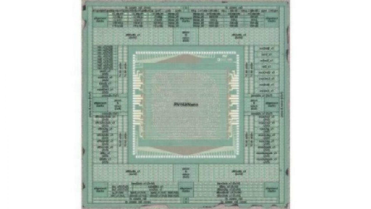
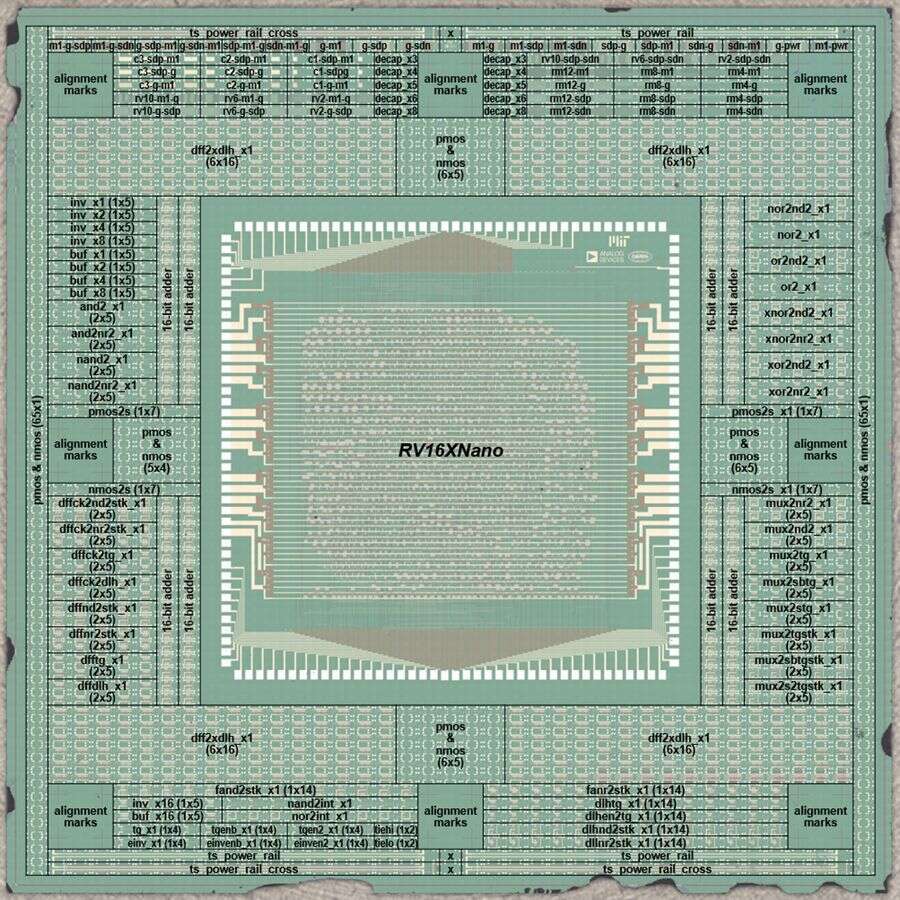
The 16-bit microprocessor is based on the RISC-V instruction set, runs standard 32-bit instructions on 16-bit data and addresses, comprises more than 14,000 complementary metal–oxide–semiconductor CNFETs and is designed and fabricated using industry-standard design flows and processes. In the paper, they propose a manufacturing methodology for carbon nanotubes, a set of combined processing and design techniques for overcoming nanoscale imperfections at macroscopic scales across full wafer substrates.
Beyond silicon, beyond Moore’s Law
The industry has to date been following Moore’s Law, shrinking and cramming more transistors onto chips every couple of years to carry out increasingly complex computations. But there will come a time when silicon transistors will stop shrinking and become increasingly inefficient. Research indicates CNFETs have properties that promise around 10 times the energy efficiency and far greater speeds compared to silicon. But when fabricated at scale, the transistors often come with many defects that affect performance, so they remain impractical.
The MIT researchers invented new techniques to dramatically limit defects and enable full functional control in fabricating CNFETs, using processes in traditional silicon chip foundries. Their CNFET based microprocessor based on the RISC-V open-source chip architecture was able to execute the full set of instructions accurately. It also executed a modified version of the classic “Hello, World!” program, printing out, “Hello, World! I am RV16XNano, made from CNTs.”
“This is by far the most advanced chip made from any emerging nanotechnology that is promising for high-performance and energy-efficient computing,” said co-author Max M. Shulaker, the Emanuel E Landsman Career Development Assistant Professor of Electrical Engineering and Computer Science (EECS) and a member of the Microsystems Technology Laboratories. “There are limits to silicon. If we want to continue to have gains in computing, carbon nanotubes represent one of the most promising ways to overcome those limits. The paper completely re-invents how we build chips with carbon nanotubes.”
Buy carbon nanotubes off-the-shelf, drop them onto a wafer, build the circuit
The microprocessor builds on a previous iteration designed by Shulaker and other researchers six years ago that had only 178 CNFETs and ran on a single bit of data. Since then, Shulaker and his MIT colleagues have tackled three specific challenges in producing the devices: material defects, manufacturing defects, and functional issues.
For years, the defects intrinsic to carbon nanotubes have been a “bane of the field,” Shulaker says. Ideally, CNFETs need semiconducting properties to switch their conductivity on an off, corresponding to the bits 1 and 0. But unavoidably, a small portion of carbon nanotubes will be metallic, and will slow or stop the transistor from switching. To be robust to those failures, advanced circuits will need carbon nanotubes at around 99.999999 percent purity, which is virtually impossible to produce today.
The researchers came up with a technique called DREAM (an acronym for “designing resiliency against metallic CNTs”), which positions metallic CNFETs in a way that they won’t disrupt computing. In doing so, they relaxed that stringent purity requirement by around four orders of magnitude — or 10,000 times — meaning they only need carbon nanotubes at about 99.99 percent purity, which is currently possible.
Designing circuits basically requires a library of different logic gates attached to transistors that can be combined to, say, create adders and multipliers — like combining letters in the alphabet to create words. The researchers realized that the metallic carbon nanotubes impacted different pairings of these gates differently. A single metallic carbon nanotube in gate A, for instance, may break the connection between A and B. But several metallic carbon nanotubes in gate B may not impact any of its connections.
In chip design, there are many ways to implement code onto a circuit. The researchers ran simulations to find all the different gate combinations that would be robust and wouldn’t be robust to any metallic carbon nanotubes. They then customized a chip-design program to automatically learn the combinations least likely to be affected by metallic carbon nanotubes. When designing a new chip, the program will only utilize the robust combinations and ignore the vulnerable combinations.
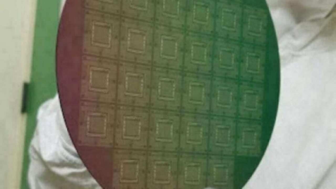
RV16X-NANO 150-mm wafer built
from complementarycarbon nanotube transistors.
Each wafer includes 32 dies .
“The ‘DREAM’ pun is very much intended, because it’s the dream solution,” Shulaker says. “This allows us to buy carbon nanotubes off the shelf, drop them onto a wafer, and just build our circuit like normal, without doing anything else special.”
Exfoliating and tuning
CNFET fabrication starts with depositing carbon nanotubes in a solution onto a wafer with predesigned transistor architectures. However, some carbon nanotubes inevitably stick randomly together to form big bundles — like strands of spaghetti formed into little balls — that form big particle contamination on the chip.
To cleanse that contamination, the researchers created RINSE (for “removal of incubated nanotubes through selective exfoliation”). The wafer is pretreated with an agent that promotes carbon nanotube adhesion. Then, the wafer is coated with a certain polymer and dipped in a special solvent. That washes away the polymer, which only carries away the big bundles, while the single carbon nanotubes remain stuck to the wafer. The technique leads to about a 250-times reduction in particle density on the chip compared to similar methods.
Lastly, the researchers tackled common functional issues with CNFETs. Binary computing requires two types of transistors: “N” types, which turn on with a 1 bit and off with a 0 bit, and “P” types, which do the opposite. Traditionally, making the two types out of carbon nanotubes has been challenging, often yielding transistors that vary in performance. For this solution, the researchers developed a technique called MIXED (for “metal interface engineering crossed with electrostatic doping”), which precisely tunes transistors for function and optimization.
In this technique, they attach certain metals to each transistor — platinum or titanium — which allows them to fix that transistor as P or N. Then, they coat the CNFETs in an oxide compound through atomic-layer deposition, which allows them to tune the transistors’ characteristics for specific applications. Servers, for instance, often require transistors that act very fast but use up energy and power. Wearables and medical implants, on the other hand, may use slower, low-power transistors.
The main goal is to get the chips out into the real world. To that end, the researchers have now started implementing their manufacturing techniques into a silicon chip foundry through a program by DARPA, which supported the research. Although no one can say when chips made entirely from carbon nanotubes will hit the shelves, Shulaker says it could be fewer than five years. “We think it’s no longer a question of if, but when,” he said.

Subscribe to Newsletter

Test Qr code text s ss
