Excitons Pave the Way to Future Electronics
Article By : Nitin Dahad
After developing a method to control exciton flows at room temperature, EPFL scientists have discovered new properties of these quasiparticles that can lead to more energy-efficient electronic devices.
LONDON — A laboratory in Switzerland has found a way of using a laser to change and regulate the polarization, wavelength and intensity of light in "excitons" in 2D materials, creating the potential for a new generation of transistors with less energy loss and heat dissipation, opening up the potential for low-power quantum computing.
Excitons are created when an electron absorbs light and moves into a higher energy level, or "energy band" as it is called in solid quantum physics. This excited electron leaves behind an "electron hole" in its previous energy band. And because the electron has a negative charge and the hole a positive charge, the two are bound together by an electrostatic force called a Coulomb force. It’s this electron-electron hole pair that is referred to as an exciton.
Scientists from EPFL’s Laboratory of Nanoscale Electronics and Structures (LANES) had already developed a method to control exciton flows at room temperature last year. In the latest development, they have discovered new properties of these quasiparticles that can lead to more energy-efficient electronic devices and have found a way to control some of the properties and change the polarization of the light they generate. The scientists’ discovery forms part of a relatively new field of research called valleytronics and has just been published in Nature Photonics.
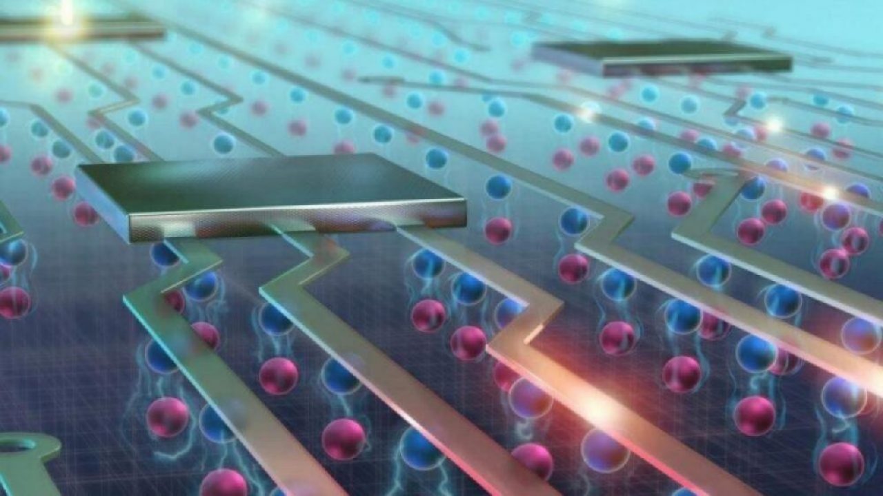
Excitons exist only in semiconducting and insulating materials. Their extraordinary properties can be easily accessed in 2D materials, whose basic structure is just a few atoms thick. The most common examples of such materials are carbon and molybdenite. When such 2D materials are combined, they often exhibit quantum properties that neither material possesses on its own.
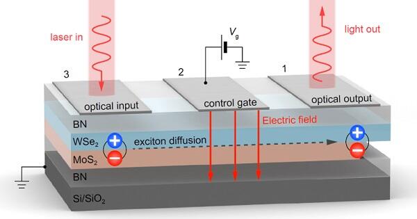
The diagrammatic structure of the exciton device. (Source: EPFL)
The EPFL scientists thus combined tungsten diselenide (WSe2) with molybdenum diselenide (MoSe2) to reveal new properties with an array of possible high-tech applications. By using a laser to generate light beams with circular polarization, and slightly shifting the positions of the two 2D materials so as to create a moiré pattern, they were able to use excitons to change and regulate the polarization, wavelength and intensity of light.
This is achieved by manipulating one of the excitons’ properties: their “valley,” which is related to the extremes of energies of the electron and the hole. These valleys — which is where the name valleytronics comes from — can be leveraged to code and process information at a nanoscopic level.
“Linking several devices that incorporate this technology would give us a new way to process data," said Andras Kis, the lead scientist at the EPFL lab. "By changing the polarization of light in a given device, we can then select a specific valley in a second device that’s connected to it. That’s similar to switching from 0 to 1 or 1 to 0, which is the fundamental binary logic used in computing.”
Valleytronics Opens up Edge and Quantum Computing
A research team in Singapore is also looking at the potential for valleytronics and particularly its likely use in quantum computing. Singapore-based researcher Johnson Goh and his team from the A * Star Institute of Materials Research and Engineering are hoping to demonstrate in early 2019 their first proof-of-concept of devices that use valleytronics to do simple things, such as switch a device on or off. In a recent report, he said that a combination of valleytronics and 2D materials will enable new functionalities in nanoelectronic and nanophotonic devices that can’t be achieved with existing silicon-based semiconductor technology. In particular, it would allow electron transport in 2D materials to be manipulated at lower energies than conventional devices.
Goh and his colleagues are looking to address a major obstacle in the commercialization of this technology; for large scale electronics production this would necessitate forming 2D materials with uniform thickness and electrical properties on at least a four-inch wafer. The method being considered for manufacturing large-area 2D semiconductor materials is chemical vapor deposition.
He said that if the valley electrons are put into superposition states, they could produce a qubit — the fundamental unit for quantum computing. This could be the biggest area for valleytronics, especially for low-power edge computing and eventually quantum computing, he added.

Subscribe to Newsletter

Test Qr code text s ss
