New DRAM Architecture Targets Edge AI
Article By : Junko Yoshida

Etron Technology revealed a brand-new DRAM architecture called “Reduced Pin Count” (RPC) DRAM, which uses only half the pins to drive miniaturization and cut cost...
LAS VEGAS — Over the last few decades, the DRAM industry has single-mindedly followed a single roadmap in pursuit of higher-density memories, beginning with asynchronous DRAM and evolving to DDR5 synchronous DRAM.
In contrast, Etron Technology (Hsinchu, Taiwan) revealed at the Consumer Electronics Show that instead of following the conventional path, it's charting an alternative roadmap with a brand-new DRAM architecture called “Reduced Pin Count” (RPC) DRAM.
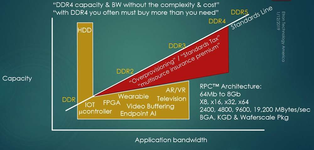
With RPR DRAM, the DRAM roadmap can diverge (Source: Etron)
Etron CEO Nicky Lu argued that the proposed RPC DRAM, which uses only half the pins, can both drive miniaturization and cut cost. He pitched PRC DRAM as ideal for miniaturized wearable devices and end-point AI subsystems. With DDR4, many companies designing small wearable devices today must buy more than they need, Lu added. “For many designers of small systems, DDR4 is an overkill.”
More specifically, Etron’s RPC DRAM features x16 DDR3 bandwidth, but uses only 22 switching signals in a 40-ball fan-in Wafer Level Chip Scale Package (FI-WLCSP). RPC DRAM will offer “DDR4 capacity and bandwidth without the complexity and cost,” Etron claimed.
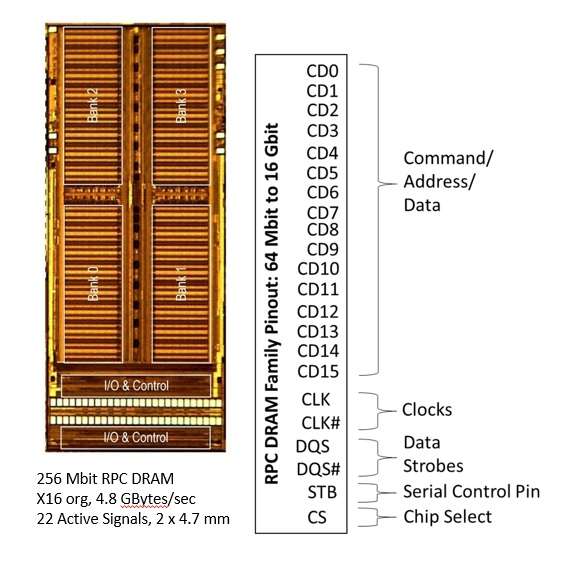
RPC DRAM is similar to a DDR3 or LPDDR3 DRAM but has less than half the pins (Source: Etron)
RPC for under-served market
Jim Handy, an analyst at Objective Analysis, told EE Times, “Something interesting about DRAMs is that the major manufacturers focus solely on the parts that sell in hundreds of millions and billions of units per year.” He observed, “This creates opportunities for companies like Etron, provided they can put in the effort to define the markets that aren’t well served by commodity DRAM and produce parts that satisfy the needs of those markets. This is an example.”
Asked what problems RPC DRAM is designed to solve, Handy said, “This is mostly about saving money and/or space.” He noted, “Etron makes a compelling argument that RPC will save costs in both the DRAM (by allowing companies to buy lower-density parts) and FPGAs or SoCs by reducing the number of I/O pins or otherwise supporting smaller logic die sizes.”
Handy added, “I always find cost savings to be the most compelling argument for any new product.”
RPC DRAM isn’t just a “concept” of new DRAM architecture. At CES, Etron disclosed that it is already collaborating with Lattice Semiconductor to demonstrate the interoperability of Lattice’s EPC5 FPGA solution and Etron’s RPC DRAM.
Etron-Lattice collaboration
EE Times asked Lattice what the FPGA company has found “unique” or “beneficial” in RPC DRAM architecture that it can’t get from conventional DRAM.
Gordon Hands, director, product marketing at Lattice, told us, “Users of many chips including FPGA place a high premium on I/O pins. They are often the limiting resource for designers. By eliminating the need for separate control and address pins, the Etron RPC memory conserves this scarce resource.”
Is there anything about Lattice’s FPGA that makes it more convenient to adopt RPC DRAM?
Hands explained, “Since the inception of the ECP brand, Lattice has focused on providing more FPGA bandwidth per logic capacity than other mid-ranged value FPGAs. This is delivered with predesign elements in the I/O ring that make it possible for designers to implement DDR memory interfaces. We reused these elements to support the Etron RPC.”
To date, the Lattice-Etron collaboration has created a “a proof of concept design that verifies Lattice and Etron silicon interoperates,” said Lattice’s Hands. During the first half of 2019, Lattice hopes to release “a series of reference designs and demonstrations that will accelerate customer design implementation using this technology,” he added.
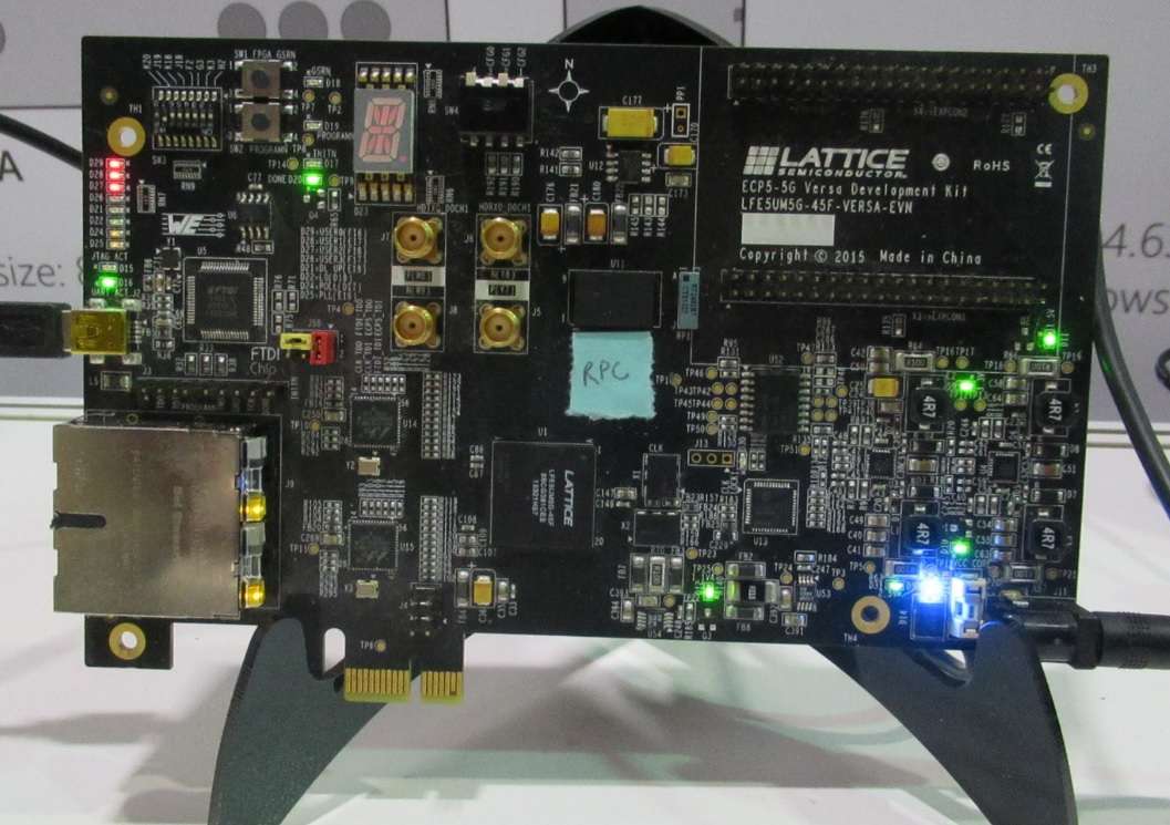
Lattice's FPGA and Etron's RPC SRAM on a reference board shown at CES (Photo: EE Times)
No alternatives to RPC DRAM?
So, how badly is this type of new memory architecture needed by OEMs and ASIC designers? Are there alternative solutions to RPC DRAM?
Objective Analysis’ Handy said, “Right now, designs that don’t need the large density of existing DRAM will often use an SRAM, but that’s pretty costly.” He noted, “Low-density DRAMs are another option, but they use wider interfaces than are required by most designs.”
In Handy’s opinion, “RPC promises to… replace both of these with a more cost-effective solution. As long as Etron follows through, they should be able to do well.”
The size of memory matters
Miniaturization is a critical factor in wearable devices, a reality that makes memory size the big drawback, noted Etron’s Lu.

Lu cited the example of smart eyeglasses, such as Google Glass. He explained that DDR3 bandwidth is sufficient for such smart eyeglasses to do video capture and playback. The problem, Lu said, is that a 9×13 mm ball grid array (BGA) of DDR3 won’t fit into the glasses.
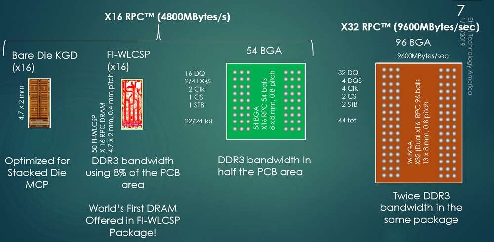
Lu said DDR3 memory comes in an x16 configuration in a 96-ball BGA package approximately 9 x 13 mm. No matter what the die capacity, the minimum package size remains the same, set by the standardized ball footprint of six columns of 16 balls using a 0.8 mm pitch. Within a wide range of die capacities (256 Mbit to 8 Gbit) the same BGA package is used.
But what if DRAM is offered other than BGAs?
Fan-In Wafer Level CSP (FI-WLCSP) packages are manufactured differently from BGAs, Lu explained. Instead of assembling one package at a time, “an entire wafer is packaged in a batch.” Each packaged unit is the size of the semiconductor die: A small die results in a small FI-WLCSP package. Lu claimed, “RPC DRAM is the world’s first DRAM offered in a FI-WLCSP package.”
RPC DRAM comes in different packaging (Source: Etron)
With an FI-WLCP package, there is no substrate and there are no wire-bonding or flip-chip assembly steps. Package assembly consists of additive steps comprising deposited dielectrics and conductors that are photo-defined, followed by electroplating and solder ball drop. All processing happens on full wafers.
Richard Crisp, vice president and chief scientist for imaging and memory product development at Etron, told EE Times that “the reduced pin count and small die size are the key factors allowing this RPC DRAM to be placed into a FI-WLCSP.” He stressed, “No other DRAM is offered in this package anywhere: it’s the size of a grain of rice.”
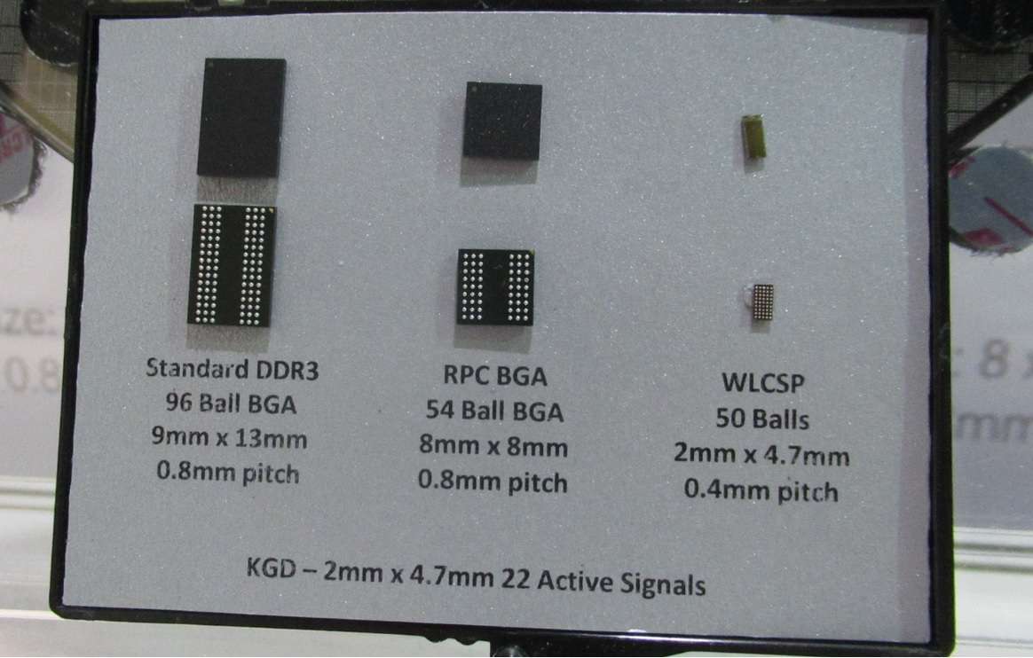
Size comparison: Standard DDR3 in BGA vs. RPC DRAM in BGA and in FI-WLCSP (Photo: EE Times)
It’s all about cost
So, to promote the adoption of RPC DRAM throughout the market, what must Etron do? Objective Analysis’ Handy said, “They need to make sure that they price it in a way that provides a net cost benefit to the OEM. They seem to already be focused on this, so they’ve embarked on the right path.” He added, “It would probably help if they lined up alternate sources of supply for those OEMs who might be skittish of depending on a single source of supply.”
Asked about RPC DRAM foundries, Etron told us the company uses the same foundries as for Etron’s other DRAMs with same sourcing arrangements but declined to name them. Asked about RPC DRAM production, Etron’s Crisp stressed, “We do all this with standard processing and materials and no ‘heroic’ signaling or exotic materials compared to standard DDR3.”

Subscribe to Newsletter

Test Qr code text s ss
