(Step-by-Step) Design for EMI Test
Article By : Rohde & Schwarz
Improve your time to market, no more missing your NPI deadlines due to EMI compliance
Before you begin…
Setup your scope for EMI debugging by selecting the right frequency band and resolution bandwidth
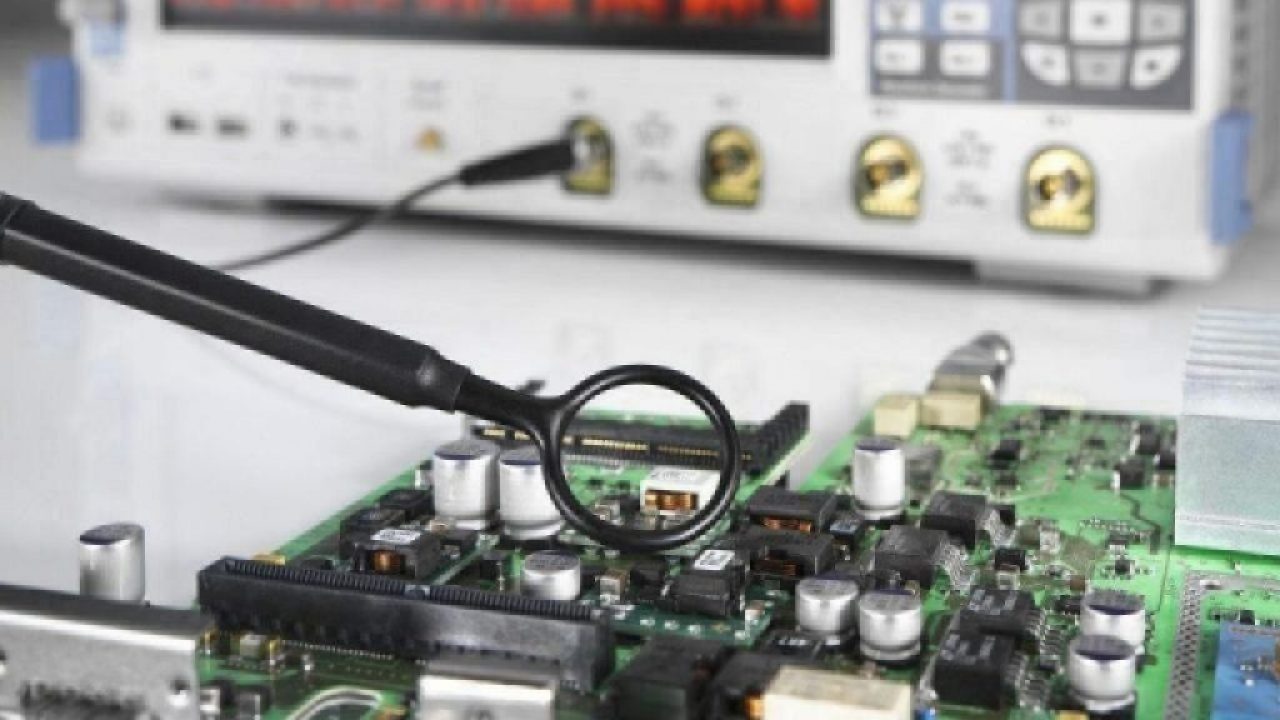
Step 1: Locate the culprit
Search and locate the EMI sources on PCB with a nearfield probe. Observe both the time and frequency characteristics. Within the same scope, view simultaneous FFT on specific period. Intensity grading helps you to visualize and understand the possibility of interference.
Step 2: Capture the emissions
Check if interference exist by using the gated FFT function during transmitting and non-transmitting scenario. Make full use of your scope with time domain trigger, zone trigger, mask violation, serial, parallel and protocol trigger…
Step 3: Analyze the behavior of the interference
Correlate unwanted emissions with time domain events with gated FFT. You may want to overlay multiple FFT to make better sense of correlation. Is your signal narrowband or broadband? Analyze both signals with different strategies.
Download the free EMI step-by-step e-guide HERE.
Save the Date (18 Jan 2019) — Rohde & Schwarz will hold an EMI seminar titled “Uncover and solve the hidden EMC issue” on 18 Jan 2019 in Singapore. Together with industry partners, Würth Electronics and Dassault Systemes Simulia CST, the session will focus on shielding effectiveness. For more details and registration, click here.
For further enquiries, email to event.apac@rohde-schwarz.com.
Explore also:
- From the industry experts to you: detect EMC issues early!
- Wide bandgap semiconductor switches optimization for EMI compliance

Subscribe to Newsletter

Test Qr code text s ss
