Wide bandgap semiconductor switches optimization for EMI compliance
Article By : Rohde & Schwarz
Correlated time-frequency measurements optimizes gate driving and minimize EMI emission
The
wide bandgap materials such as silicon carbide (SiC) and gallium nitride (GaN)
for semiconductor switches are able to operate at high switching frequencies
with steep rising edges and high voltage. These characteristics enhance the
efficiency of switching power supplies but at the same time increase the
challenges for EMI compliance. Optimizing for EMI compliance during development
phase would reduce effort needs at later stage.
One
source of EMI emission is the fast switching MOSFET bridge. A direct approach
to reduce EMI is to modify the gate driving voltage of the switching
transistors. This requires parallel measurement of the gate driving voltage,
the output signal and the emitted radiation, as well as their spectrum.
|
|
|
|
(a) |
(b) |
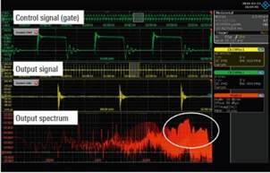
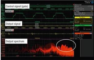
Figure
1: Various drive signals of MOSFET bridge and their effect on emitted
radiation. © IFE Graz University of Technology Austria
In
Figure 1, the EMI emission of MOSFET bridge (red) is significantly reduced by
optimizing the gate driving voltage (green). Observing the green waveforms,
1(a) uses a rectangular gate drive signal while 1(b) uses a cascaded two-level
gate drive signal. EMI emission is observed in parallel with a near field
probe. It clearly shows the amplitude of high frequency components in EMI signal
(red) is reduced effectively.
The
test solution
Rohde
& Schwarz oscilloscopes have direct frequency and resolution bandwidth
input and fast update rate. Combining with the R&S®HZ-15 compact probe set
for E and H near-field measurements and R&S®HZ-17 compact H near field
probe set (both 3GHz bandwidth), the source and transmission path of unwanted
emissions on a PCB can be easily located.
To
learn more on this EMI emission test and further optimization steps, click here.
Explore
also: From
the industry experts to you: detect EMC issues early!

Subscribe to Newsletter

Test Qr code text s ss
