ISSCC Sees AI, 5G and Big Memories as Talking Points
Article By : Rick Merritt
This year’s International Solid-State Circuits Conference sees Toshiba outline a 1.33 Tbit NAND chip, among others
SAN JOSE, Calif. — Forget Moore’s Law and screaming microprocessors. This year’s International Solid-State Circuits Conference (ISSCC) is all about the age of data in which machine learning, fast networks, and fat memories are king.
Samsung and Intel will detail 5G/LTE combo chips. In NAND flash, Toshiba will describe a 1.33-Tbit chip, and Western Digital will talk about a 128-layer one. In DRAM, SK Hynix and Samsung will report on DDR5 and LPDDR5. Separately, Samsung will present a deep-learning accelerator for smartphones.
This year’s event has no papers on 5-nm SRAMs or test chips, although it does include talks on a handful of fast 7-nm networking chips. In another break from the past, there are no papers on flagship CPUs.
“We do not believe this will be a continuing trend but, rather, an indication of where the industry is in terms of product cycles,” wrote an organizer of the microprocessor session.
In their place, ISSCC invited IBM engineers to describe the Summit and Sierra supercomputers, currently the most powerful systems in the world. The processor session also hosts an interesting paper on a robot controller that scales from 37 to 238 mW at 80–365 MHz using an Intel 22-nm process intended as a rival to fully depleted silicon-on-insulator.
Staking out the new reality, Yann LeCun, director of AI research at Facebook, will give the opening keynote. The father of convolutional neural networks will describe the road to unsupervised learning, where machines learn like people do from their environment.
AI and 5G will also be topics of all-day tutorials and short courses that book-end the start and end of the conference.
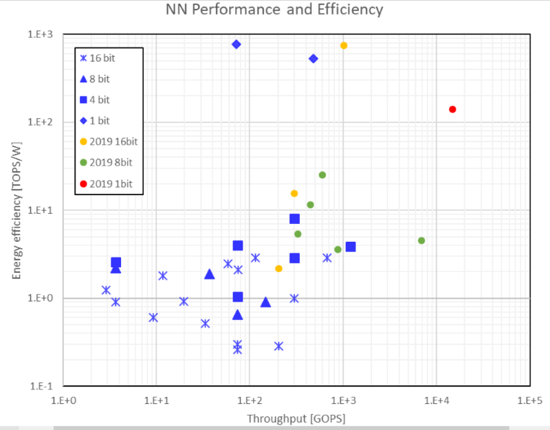
Organizers provided context on progress on the efficiency and throughput of deep-learning processors for CNNs/DNNs presented at ISSCC 2019 compared to the state of the art in 2018. Click to enlarge. (Source: ISSCC)
Samsung’s mobile accelerator for deep learning delivers up to 11.5 tera-operations/second (TOPS) at 0.5 V and fits into 5.5 mm2 in an 8-nm process. It packs 1,024 multiply-accumulate units in a dual-core design and delivers a tenfold performance boost over the previous state of the art, said ISSCC organizers.
Toshiba will describe a 16-nm SoC for robocars that delivers 20.5 TOPS in a 94.52-mm2 die that includes 10 processors, four DSPs, and eight accelerators. It performs ASIL-B–compliant image recognition and ASIL-D–compliant control processes.
In a session on in-memory computing, a hot approach in AI acceleration, National Tsing Hua University will detail a chip that delivers 53.17 TOPS/W in binary mode using resistive RAM. The device sports an operation latency of 14.6 ns.
In fast networks, Samsung and Intel will go head to head describing rival transceivers that handle 5G and LTE cellular.
Samsung will detail a 14-nm, 38.4-mm2 chip that supports 2G, 3G, LTE, and both standalone and non-standalone 5G modes. It uses 14 receive and two transmit paths to deliver up to 3.15 Gbits/s down and 1.27 Gbits/s up.
In related papers, Samsung will present a power supply modulator for sub-6-GHz 5G networks, supporting 100-MHz bandwidth for envelope tracking and offering an 88% efficiency. It will also detail a power management IC for a 5G millimeter-wave transceiver capable of 90 ns/V and 110 ns/V for up- and down-tracking.
The chips are part of Samsung’s Exynos Modem 5100, a 5G chipset supporting both sub-6-GHz and mmWave networks to be shown at an ISSCC demo event. Together, the chips show that the Korean giant expects to deliver serious competition to market leader Qualcomm in 5G.
It is not alone. Intel will present a 28-nm 4G/5G transceiver for sub-6-GHz bands in zero-IF and 10.56-GHz IF for mmWave bands. It sports an M-PHY Gear 3 interface for MIMO and up to 800-MHz bandwidth with carrier aggregation. It is part of a 5G chipset that Intel announced earlier this month.
Wired networks are also stepping on the gas. Huawei, eSilicon, Mediatek, and IBM will show 7-nm devices delivering data rates up to 128 Gbits/s, generally using PAM-4 modulation that, a few years ago, was the subject of lively debates among engineers over whether it was commercially viable.
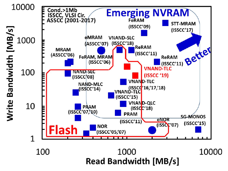
Organizers compared historical trends of read/write bandwidth for non-volatile memories. Click to enlarge. (Source: ISSCC)
Filling the data age’s hunger for storage, Toshiba will present a 1.33-Tb, 4-bit/cell (QLC) 3D-NAND chip using a 96-layer design 3D-NAND. It packs 8.5 Gbits/mm2.
Rival Western Digital will detail a 512-Gbit, 3-bit/cell chip using a record 128-layer stack. It places control circuits under the memory array and delivers a write throughput of 132 MBytes/s.
For its part, Samsung will show a 512-Gbit 3-bit/cell chip delivering 1.2 Gbits/s. It reduces worldline and bitline setup times to boost read and write performance.
In embedded memories, Intel will demonstrate advances in ReRAM and MRAM for its 22-nm FinFET node. Organizers said that the 10.1-Mb/mm2 ReRAM macro is a viable candidate for next-generation MCUs given its relatively low cost and high speed. A 7-Mbit STT-MRAM uses a write-verify-write scheme and offset cancellation sensing.
In DRAM, the event will host some of the first technical talks about next-generation devices.
Samsung will present a 10-nm–class LPDDR5 chip. It reduces read and write power consumption by 21% and 33%, respectively, compared to LPDDR4X by using dynamic voltage frequency scaling and a deep-sleep mode. The memories are expected to see use in 5G designs, advanced driver assistance systems, high-resolution displays, and mobile devices.
For its part, SK Hynix will describe a 16-Gbit DDR5 SDRAM that delivers 6.4 Gbits/s/pin. Energy efficiency is improved more than 30% over the prior DDR4.
As always, the ISSCC horizon is broad. Papers span the range from analog and power devices to medical implants and devices for quantum computers.
In radar for robocars, Mediatek will describe a 79-GHz transceiver that fits in a 16 × 25-mm package. Startup Uhnder will detail a 77-/79-GHz MIMO radar SoC made in a 28-nm process that supports 6-cm range, 1° angular and 0.099-km/h Doppler resolutions. And Intel will describe a 71- to 76-GHz 64-element phased-array transceiver made in its 22-nm process.
Researchers from four universities will present a millimeter-scale ultrasound ASIC that can be inserted into the human heart to track its structure in real time. It aims to be used to guide for a specific form of therapy called atrial septal defect closure.
Just for fun, organizers invited engineers from Sony to give a paper on their recently re-released robotic dog, the Aibo. At the wild and hairy fringe, researchers from Google and two universities teamed up to design a 28-nm chip that controls superconductive qubits using 4- to 8-GHz signal patterns operating at deep-cryogenic temperatures.
— Rick Merritt, Silicon Valley Bureau Chief, EE Times

Subscribe to Newsletter

Test Qr code text s ss
