GlobalFoundries Progressing with FD-SOI AI Chips
Article By : Rick Merritt

New deep learning projects on enhanced existing processes after 7nm failure
SANTA CLARA, Calif. — In its first annual conference since halting work on 7 nm, Globalfoundries described a handful of enhancements to its existing nodes. It also showcased a new customer making at least three embedded deep-learning chips in its 22-nm fully depleted silicon-on-insulator process.
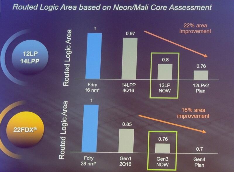
GF promised to squeeze out 10% to 22% area, performance, and power gains from its 12-/14-nm FinFET and planar nodes. That’s roughly in line with the kind of gains that its much larger rival, TSMC, is reporting in bleeding edge nodes as Moore’s Law slows.
Synaptics announced that it taped out at GF a low-power 22-nm FD-SOI accelerator for neural networking. It sports tera-operations/second performance using AI technology licensed from an unnamed source. The company plans to tape out in the node a second voice/video chip before the end of the year and a third for AR/VR in early 2019.
It’s a small step from a company that dominates touchscreen chips and buys 500,000 wafers/year. Likely far fewer than a quarter of those wafers will come from GF in the next couple of years, but the move validates that the node is well-positioned for one of the industry’s hottest markets.
“We went through an extensive review and found that 22-nm FDX is a good fit for AI-enabled IoT products” with more performance and less active power than 28-nm planar and less cost than FinFETs, said Synaptics CEO Rick Bergman.
Tom Caufield said that visits with European chip vendors such as Bosch, Infineon, and NXP after he was named GF’s chief executive in March helped show the way. They provided role models in stepping back when returns slowed for chips designed on bleeding edge nodes, he said.
“The vast majority of our customers have no intention to use something below 10 nm in their lifetimes … [while his only 7-nm prospects, AMD and IBM, said that] you will always be late and your [leading-edge] capacity is too small for us,” he said in a frank keynote.
The foundry, which had risen to a $6 billion business in 2017, would have had to spend $3 billion — half of it raised from outside investors — to install even a modest capacity of about 30,000 7-nm wafers/month. “The returns would be like CD returns … it was time for us to become more relevant,” he said.
Advances claimed in FinFETs, RF, and libraries
Now GF is focused on delivering 15% more density and 10% more performance on its 12-nm process compared to its 14-nm node. Over three generations, library enhancements and other techniques could push density up 22% and power down 25% and deliver 18% more density in planar nodes, claimed the company.
The 22-nm FD-SOI node now sports 55 design wins valued at $2 billion across a variety of markets and regions. However, two-thirds of the chips won’t be in GF’s Dresden fab until the first half of next year.
A follow-on 12-nm FD-SOI is yielding 90% of its target performance, said CTO Gary Patton. He described one 22-nm design as a single-chip LTE baseband with integrated direct conversion and power management using 36 masks.
In packaging, GF supports automated fiber alignment for silicon photonics as well as silicon interposers capable of handling four HBM stacks. It also supports an RF package that integrates antennas, he said.
Separately, GF has its 8SW RF SOI node in production on 300-mm wafers for designs such as sub-6-GHz RF cellular front ends. It lowers power as much as 70% and size by 20% compared to the former node.
Caulfield promised that GF will spend more than $1 billion a year on capex while increasing free cash flow up to 15%.
Both attendance and partnerships were on the rise at the event, GF claimed. Its FD-SOI program now sports 52 partners, and a new RF partner program includes 14 design and tool companies.
Among its new partners, Imagination Technologies showed working Bluetooth Low Energy and 802.15.4 parts made in GF’s 22-nm node. The IP cores are available now, but merchant parts will come next year after a respin.
In the past year, GF shed more than a thousand employees in layoffs in June and August under Caulfield. Nevertheless, the company has “a shot at being commercially successful,” said analyst Nathan Brookwood of Insight64. “The new requirements of IoT seem to be well-aligned with its FD-SOI technology.”
— Rick Merritt, Silicon Valley Bureau Chief, EE Times

Subscribe to Newsletter

Test Qr code text s ss
