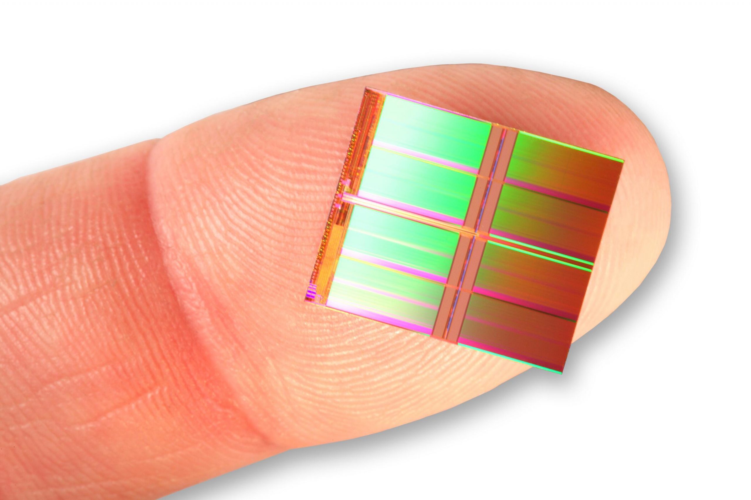
The Latest in NAND
Article By : Rick Merritt
Rick Merritt summarizes the Flash Memory Summit
SAN JOSE, Calif. — Four established 3D NAND flash makers showed at least small pieces of their roadmaps in keynotes at the Flash Memory Summit here. Their latest rival, Yangtze Memory Technology Corp. (YMTC), gave a deeper dive into its technology and business outlook in a meeting with press.
SK Hynix was the most forthcoming of the established players, providing details of its 96-layer devices. Toshiba announced a low-latency chip geared to compete with Samsung’s Z-NAND and Intel’s Optane. Micron only gave a brief glimpse of its next-generation plans, and Western Digital rolled out new software as part of a data center strategy.
The news comes at a time when hard disk drives still dominate computer storage. However, NAND flash is on a tear, expected to make up as much as half the market by 2025, according to some market projections.
SK Hynix announced that it will sample before the end of the year a 512-Gbit version of its 96-layer chips in an 11.3 x 13-mm2 package for mobile systems. Before June, it will sample a Tbit version of its so-called V5 family in a 16 x 20-mm2 package. Both chips use a charge-trap architecture and support data rates up to 1.2 Gbits/s/pin.
The V5 parts are 30% smaller than its current 72-layer NAND chips. They provide a 25% boost in read and 30% boost in write performance. Overall power efficiency is up 150% compared to its current products.
SK Hynix is already working on a next generation with 128 layers. It expects to eventually deliver chips with more than 500 layers that pack 8 Tbits into a single package, said Hyun Ahn, a senior vice president of NAND development and business strategy for the company.
For its part, the newly reformed Toshiba Memory Corp. said that it will start production early next year on a 1.33-Tbit chip. It will be a Gen 4 version of its BiCS architecture using 96 layers and 4 bits/cell.
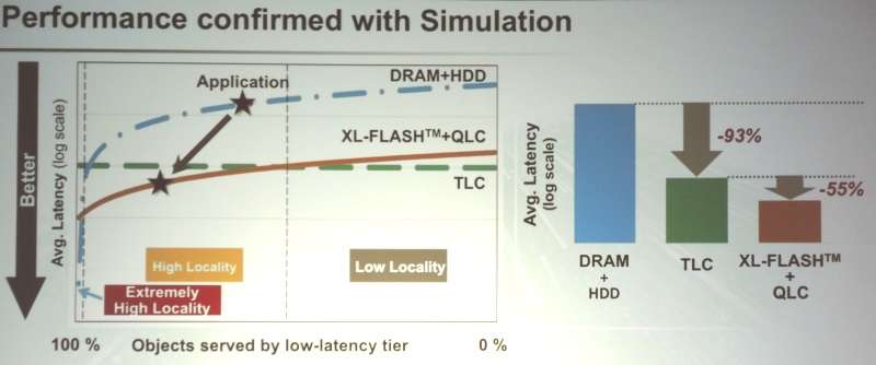
Separately, Toshiba announced XL-Flash, a chip sporting one-tenth of the random-read latency of its current 3-bits/cell parts. The component uses shorter word lines and more planes but otherwise leverages the existing BiCS process and interfaces.
The company, which claims leading market share for SATA drives, said that the interface will die off in about two years, replaced by SAS and NVMe drives. The event was a showcase for several NVMe drives using PCI Express Gen 4.
Micron, WD sparse on chip details
A Micron talk was bullish on NAND growth but said little about its roadmap. Micron recently severed its collaboration with Intel on 3D XPoint memories.
Micron’s next generation NAND will sport a 30% increase in write bandwidth and 40% decline in cost/bit compared to its current 96-layer parts. The advances will be due in part to a proprietary replacement gate and low resistance metal, said the company.
Earlier, the company said that it will deliver a Tbit chip by applying 4-bits/cell technology to its existing 3D NAND devices. It expects to scale its designs beyond 200 layers and well into the next decade, said Russ Meyer, a corporate vice president for non-volatile memory integration.
For its part, Western Digital rolled out new hard-disk and solid-state arrays and management software geared to capture a bigger share of a booming storage market in data centers. Both the systems’ mechanical designs and the new virtualization APIs will be open, said Phil Bullinger, general manager of WD’s data center group.
WD’s OpenFlex E3000 will pack up to 610 TBytes of NAND storage in a 3U system using NVMe. The D3000 will carry up to 168 TBytes of hard-disk storage in a 1U chassis riding 25-Gbit/s Ethernet.
The company expects that some large data centers will design variants of the hardware to meet their needs. They also anticipate third parties writing their own management software on top of WD’s new virtualization API.
“Storage is getting significantly more complex, so drive vendors can no longer supply a simple storage device and leave the remainder of the system design to the OEM,” said Jim Handy, veteran storage analyst at Objective Analysis.
Toshiba and several others also rolled out software to manage storage networks over Ethernet and other fabrics, generally using the NVMe protocol.
Yangtze gives a deeper dive on NAND plan
Newcomer YMTC hopes to start production in July of a 256-Gbit NAND using 64 layers and wafer bonding peripheral I/O circuits on top. If all goes well, a year later, it could be producing the approximately 100-mm2 chips at a rate of 100,000 wafers/month in the first phase of a new fab now qualifying equipment at its Wuhan, China, headquarters.
A second phase of the fab would bring total capacity to 300,000 wafers/month based on the 64L design. However, a next-generation 128-layer design with 4 bits/cell already in the works would have an even smaller die size.
The 128L chips could be ready in less than 18 months, delivering 512-Gbit or even Tbit chips depending on what die size YMTC uses. If successful, that design could propel the company to a 10% to 20% worldwide NAND market share, enough to survive the market’s famous ups and downs, said Charles Kau, a memory veteran and representative of Unigroup, a lead China investor in YMTC.
“We won’t chase scale at a loss,” vowed YMTC chief executive Simon Wang, noting that the company opted not to ship a first-generation 64-Gbit device.
Although yield and reliability were acceptable, “from a cost perspective, it was not competitive,” he said, adding that the 64L part should be at 10% to 20% of the bit density of Samsung’s latest parts and deliver 10% to 20% gross margins for YMTC.
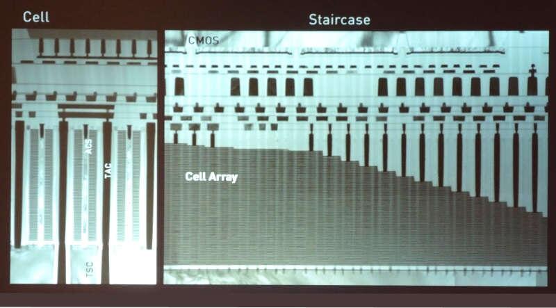
The company’s Xstacking technology is based on a wafer-bonding technique in the works for five years for CMOS imagers at the former XMC in Wuhan. YMTC pushed its “pitches at several microns” down to about 100 nm for use in 3D NAND.
To align separate NAND and I/O wafers, the trickiest part of the job, the fab uses cameras above and below the wafers along with diagnostic tools. A plasma activates the chips’ surfaces that are pressed together and annealed at low temperatures. The back side of the I/O wafer is then worked away to make pads on the back side of the die.
The approach is not expected to limit yields, which are already coming up on the 64L chip, said Yang. Reliability figures “look good,” and memory cell size and endurance are about on par with rivals.
Nevertheless, “it took some courage to go down this path because it is not easy to make this technology work … Charles and I went back and forth about the decision many times,” said Yang.
He expressed confidence that YMTC can get the equipment and materials that it needs under current export controls, the largest portion purchased from the U.S. However, he noted political risks given unpredictable decisions from the White House currently ratcheting up the heat on China trade through tariffs.
YMTC developed the Xstacking technology in-house with its more than 1,500 engineers and 500 China and international patents. It also licensed technology from Arm, IBM, Spansion, and research institutes.
In a keynote, Yang introduced himself to the event’s audience of several hundred engineers as “the new kid on the block … a good kid … we are working very hard and want to make our own contribution to the industry … hopefully, you can welcome us into this new family.”
— Rick Merritt, Silicon Valley Bureau Chief, EE Times 

Subscribe to Newsletter

Test Qr code text s ss
