Renesas Q&A: Seeing MCU Safety as Critical
Article By : Junko Yoshida, EE Times
Automotive Control Solution chief Tadaaki Yamauchi talks about the company's new MCU
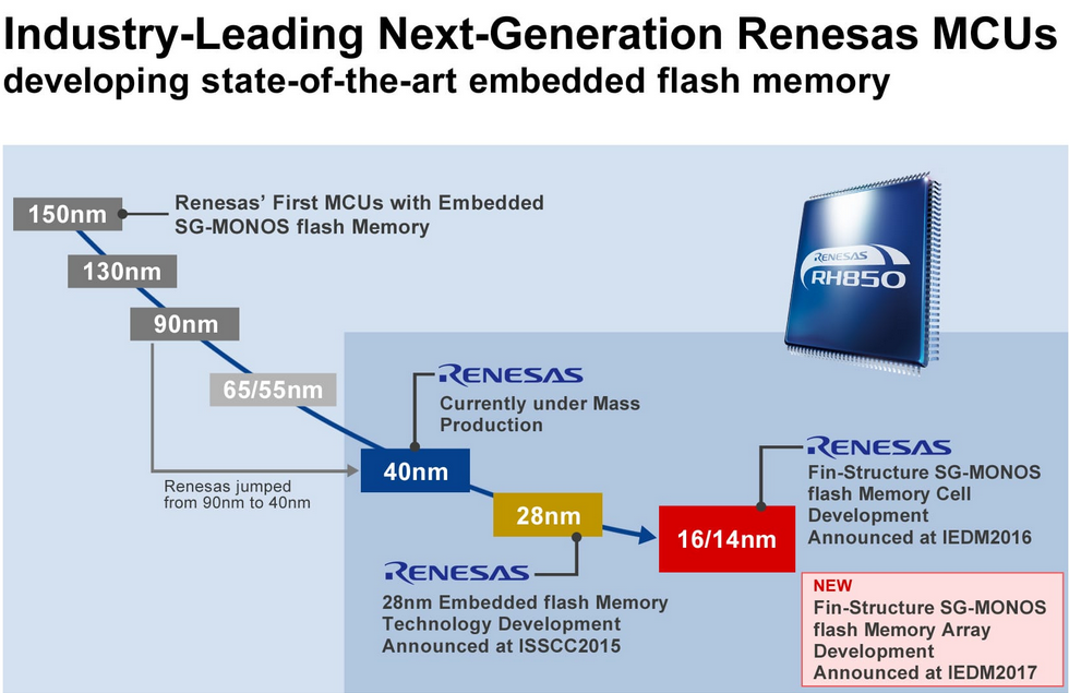
TOKYO — In efforts to boost its lofty status in the automotive MCU market share, Renesas Electronics Corp. unveiled earlier this year what it calls “the world’s first on-chip flash memory microcontroller using a 28-nm process technology.”
While tasking the company’s own R-CAR SoCs to perform sensing and cognitive functions, Renesas is counting on its automotive MCU to further penetrate the growing market of connected, autonomous, and electric vehicles.
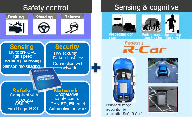
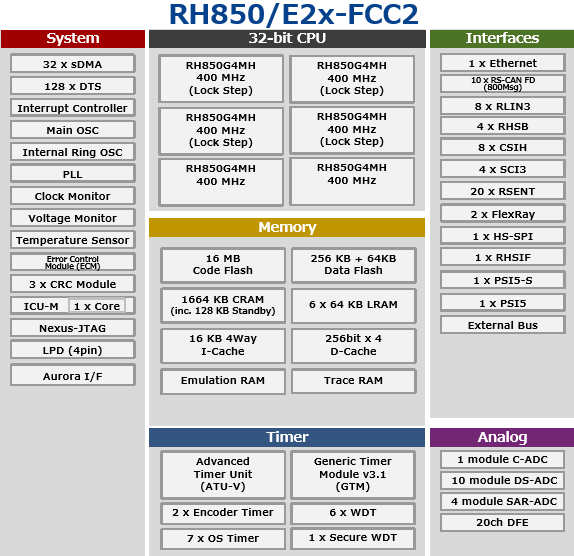
In the era of autonomous driving, the responsibility of safety MCUs is paramount. The MCU plays a crucial safety role in sensing, braking, and steering. Renesas’s new MCU, dubbed the RH850/E2x series, comes loaded with safety functions, including six 400-MHz CPU cores. Four of them, individually, are paired with their own checker CPU cores and two additional CPU cores without checkers.
Renesas has also been spending R&D resources to develop memory cell technology for the flash memory integrated into high-performance and high-reliability MCUs. While the company’s new on-chip flash memory MCU is fabricated in 28-nm process technology, Renesas claims that its team is advancing to the world’s first e-Flash Technology in leading-edge 16-/14-nm FinFET, as presented in technical papers at IEDM 2016 and 2017.
Renesas’s new MCU featuring a built-in flash memory of up to 16 megabytes (MB) is particularly important, said Renesas, now that over-the-air (OTA) software updates are poised to become prevalent in many connected vehicles.
Consider Tesla’s Model 3, subject of a new Consumer Reports assessment. The report pointed out that big flaws in Model 3 are “long stopping distance” in an emergency braking test and “difficult-to-use controls.” Responding to Consumer Reports, Tesla CEO Elon Musk decided to deploy software updates via OTA to the Model 3 fleet this weekend, triggering changes to the braking system.
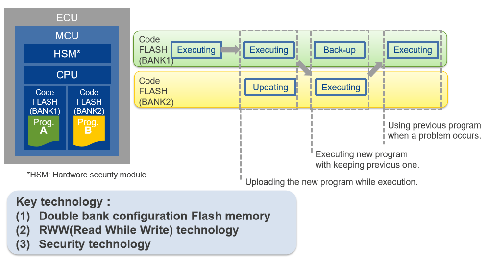
Obviously, a large memory is prerequisite to storing the new software. But what matters more is whether the flash memory is built right onto an MCU and if the built-in memory comes with two memory banks, according to Tadaaki Yamauchi, vice president at Renesas.

Speaking of OTA, he explained, “Ideally, you want to upload the new program while you are executing on it (‘no-wait OTA’).” Furthermore, he said, you want to keep the previous program “so that when a problem happens as a result of the update, you can always go back using the previous one.”
At Renesas’s headquarters here, EE Times recently caught up with Yamauchi, who now heads the company’s automotive control solution division. He used to be an engineer developing embedded flash technology. The following is part of our conversation.
EE Times: Let me first ask you about embedded flash technology. I seem to recall that, traditionally, many IDMs have tried a variety of embedded flash memory technologies, such as silicon-oxide-nitride-oxide-silicon (SONOS), silicon nanocrystal flash, SuperFlash, MirrorBit, and emFlash, among others. Which technology are you using?
Yamauchi: We are using a split-gate metal-oxide-nitride-oxide-silicon (SG MONOS) structure.
EE Times: Reportedly, one of the big challenges in embedding flash into MCUs is reliability. Many people thought that flash memory couldn’t migrate reliably or cost-effectively to 28 nm because of such issues as cell complexity and high voltages required. How confident are you with SG MONOS?
Yamauchi: Before we became Renesas, Hitachi had a 30-year history of having worked on R&D, focused on charge trap memory technology. As we continued to use MONOS eFlash for Renesas’s on-chip flash MCUs, we think we’ve proven its reliability. In collaboration with Taiwan Semiconductor Manufacturing Co., we rolled out 90-nm, 40-nm, and now 28-nm MCUs with eFlash. We pulled off the latest development because we were able to combine MONOS with TSMC’s high-performance, low-power 28-nm high-K metal gate process technology.
EE Times: Are you licensing your eFlash technology to anyone?
Yamauchi: We licensed it to TSMC for 90-nm MCUs with on-chip flash memory. Because TSMC is responsible for licensing, we aren’t sure who else has gotten that license.
EE Times: What about 40-nm MCU?
Yamauchi: We license our eFlash technology for 40-nm MCUs only for non-automotive applications. As for eFlash for 28-nm MCUs, we are not licensing it to anyone. We want to keep our lead in this segment. We also believe that SG MONOS is a good fit for further scaling.
EE Times: When did you start volume production of 40-nm MCUs with on-chip flash memory?
Yamauchi: We started sampling them in 2012 and began volume production in 2014. Our competitors are barely starting. We think we have a lead time by three to four years.
EE Times: When are you going to start the volume production of RH850/E2x series — 28-nm MCUs with eFlash?
Yamauchi: In 2020.
EE Times: Why does it take so long?
Yamauchi: This represents a whole new world for tier ones and car OEMs. It will give them enough time to develop software programs that will take advantage of large memory flash while they can also use the time to evaluate the reliability of our products.
EE Times: Who is evaluating RH850/E2x now?
Yamauchi: Our products have been already delivered to and are in the hands of a multiple number of OEMs and tier ones, including those in Japan, Europe, and the United States.
Six CPU cores inside MCU
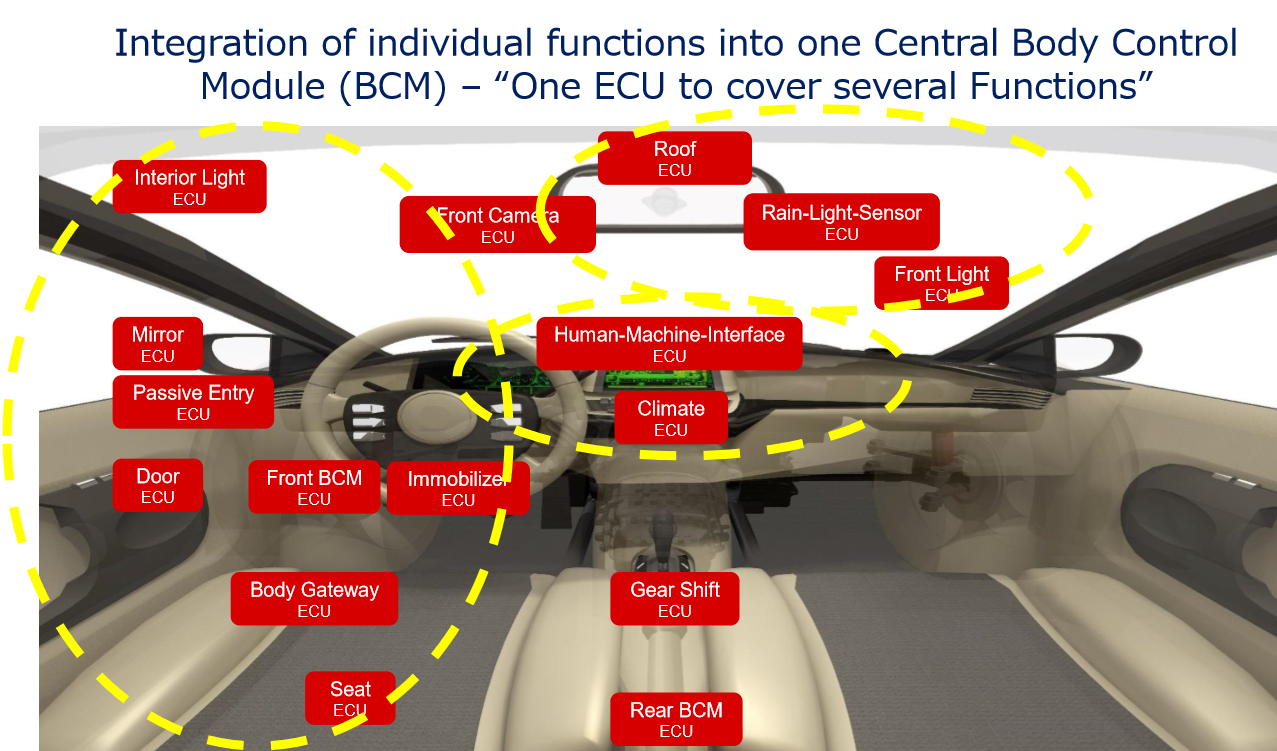
EE Times: What’s the advantage of having so many CPU cores inside RH850/E2x?
Yamauchi: In a nutshell, you can run multiple complicated processing — which has been traditionally done by several separate ECUs — on one MCU. We also improved the new MCU’s performance by three times, when compared with a 40-nm-process MCU, while keeping the power consumption at the same level [as that of the 40-nm-process MCU]. Getting the job done on one ECU instead of several ECUs also means that you can reduce harness cables that were necessary to connect them.
EE Times: Which ECU functions will be combined?
Yamauchi: We will start with what we can. The idea is for one ECU to cover several functions. The convergence of functions into one powertrain control module is one of the obvious ones.
EE Times: I’ve heard suggestions by Arm-based SoC suppliers, like Nvidia, to use hardware-enabled virtualization so that a single system can concurrently host multiple systems, such as in-vehicle infotainment systems, digital instrument clusters, and driver assistance systems.
Yamauchi: That’s different, though. Arm cores, which we also use in our R-CAR SoCs, are there to make ‘best efforts’ in their computational performance. In contrast, RH850 is there for vehicle controls. Here, we are talking about being real-time and absolute safety that matters to human lives.
EE Times: Is RH850 based on Hitachi’s SuperH core?
Yamauchi: No, its core is from NEC’s V850 — whose performance, quality, and reliability are-well tested as it’s been used in controlling engines and braking. It can withstand the most stringent real-time demands.
EE Times: When we look at the automotive MCU landscape, Mike Demler, senior analyst at The Linley Group, for example, tells me that Infineon’s Aurix MCUs are often used in the systems that he has looked at. He noted that Intel used Aurix in its Go platform, Nvidia uses Aurix in its Drive systems, and Audi uses Aurix in zFas. Aurix, too, has up to 16-MB eFlash. So what’s your advantage?
Yamauchi: First, RH850/E2x is the first MCU with eFlash fabricated in 28-nm process. Nobody else has that. Second, our SG-MONOS achieves industry’s fastest random read speed of over 120 MHz (approximately three times faster than our competitor) at low power. Third, by incorporating a compact cache memory, RH850/E2x realizes high processing performance using minimum power consumption.
EE Times: So explain to us why the next-generation MCUs need to come with built-in flash memory and how the memory is expected to be used.
Yamauchi: We see OTA functionality as the key for software-driven vehicles. OTA enables safe and secure program updating/diagnosis/recovery.
EE Times: In theory, though, you could use either discrete, external flash memory or DRAM.
Yamauchi: Obviously, discrete memory presents a cost issue. Moreover, by loading a software program first onto an external memory, it takes time before a connected vehicle can start executing it. Then there is an issue of reliability. By building a flash memory onto MCU as a single chip, we are making sure that the whole thing — memory and MCU — can stand up to heavy-duty usages under harsh automotive conditions.
EE Times: Why two memory banks?
Yamauchi: We want to make sure that users can get to use a newly updated software program without any wait. You can start executing while uploading the program. But we also want to make sure that the previous program stays in the ECU even in the event when the OTA software update fails.
EE Times: Several reports say that NXP Semiconductors has the largest share in the automotive semiconductor market. Where does Renesas stand?
Yamauchi: We hold the largest share in the automotive MCU market.
EE Times: According to whose data?
Yamauchi: Strategy Analytics. We have maintained this leading position for a while and we intend to widen the gap with our new 28-nm MCU with built-in eFlash.
Self-test diagnostic
EE Times:Since the fatal Uber accident in March, the automotive industry has been reminded of the critical importance of safety. How can you help?
Yamauchi: The quality of high-performance safety MCUs gets even more important than before. You need architecture that allows constant monitoring [checking] of hardware anomalies. Pre-requisite are enhanced self-test diagnostics by a field built-in self-test (BIST) — a mechanism that permits a machine to test itself — and enhanced fault detection. For example, we’ve gone to the extent of offering up to four sets of checker CPUs (dual-core-lockstep CPU core) in RH850/E2x.
— Junko Yoshida, Chief International Correspondent, EE Times

Subscribe to Newsletter

Test Qr code text s ss
