In-Memory Processing Making AI-Fueled Comeback
Article By : Rick Merritt
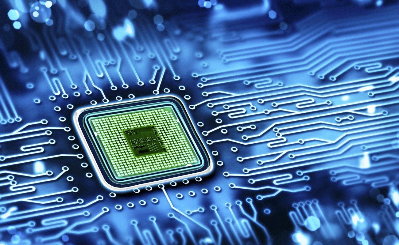
In-memory computing could propel new AI accelerators to be 10,000 faster than today's GPUs
SAN JOSE, Calif. — Startups, corporate giants, and academics are taking a fresh look at a decade-old processor architecture that may be just the thing ideal for machine learning. They believe that in-memory computing could power a new class of AI accelerators that could be 10,000 times faster than today’s GPUs.
The processors promise to extend chip performance at a time when CMOS scaling has slowed and deep-learning algorithms demanding dense multiply-accumulate arrays are gaining traction. The chips, still more than a year from commercial use, also could be vehicles for an emerging class of non-volatile memories.
Startup Mythic (Austin, Texas) aims to compute neural-network jobs inside a flash memory array, working in the analog domain to slash power consumption. It aims to have production silicon in late 2019, making it potentially one of the first to market of the new class of chips.
“Most of us in the academic community believe that emerging memories will become an enabling technology for processor-in-memory,” said Suman Datta, who chairs the department of electrical engineering at Notre Dame. “Adoption of the new non-volatile memories will mean creating new usage models, and in-memory processing is a key one.”
Datta notes that several academics attempted to build such processors in the 1990s. Designs such as the EXECUBE, IRAM, and FlexRAM “fizzled away, but now, with the emergence of novel devices such as phase-change memories, resistive RAM, and STT MRAM and strong interest in hardware accelerators for machine learning, there is a revitalization of the field … but most of the demonstrations are at a device or device-array level, not a complete accelerator, to the best of my knowledge.”
One of the contenders is IBM’s so-called Resistive Processing Unit, first disclosed in 2016. It is a 4,096 x 4,096 crossbar of analog elements.
“The challenge is to figure out what the right analog memory elements are — we are evaluating phase-change, resistive RAM, and ferroelectrics,” said Vijay Narayanan, a materials scientist recently named an IBM Research fellow, largely for his work in high-k metal gates.
Stanford announced its own effort in this field in 2015. Academics in China and Korea are also pursuing the concept.
To succeed, researchers need to find materials for the memory elements that are compatible with CMOS fabs. In addition, “the real challenge” is that they need to show a symmetrical conductance or resistance when voltage is applied, said Narayanan.
Thoughts on the future of transistors
So far, IBM has made some discrete devices and arrays but not a whole test chip with a full 4K x 4K array using what are currently seen as the ideal materials. IBM’s Geoff Burr demonstrated DNN training using phase-change materials in a 500 x 661 array that showed “reasonable accuracies and speedups,” said Narayanan.
“We are progressing steadily, we know what we need to improve in existing materials, and we are evaluating new materials.”
IBM wants to use analog elements so it can define multiple conductance states, opening a door to lower-power operation compared to a digital device. It sees a large array as an opportunity to run many AI operations in parallel.
Narayanan is optimistic that IBM can leverage its years of experience with high-k metal gates to find materials to modulate resistance in the AI accelerator. He spent a dozen years bringing IBM’s expertise in the area from research to commercial products, working with partners such as Globalfoundries and Samsung.
Looking forward, IBM is working on gate-all-around transistors that it calls nanosheets for use beyond the 7-nm node. He sees no fundamental hurdles with the designs, just implementation issues.
Beyond nanosheets, researchers are exploring negative capacitance FETs that deliver a large change in current for a small change in voltage. The idea got increased attention in the last five years, when researchers found that that doped hafnium oxide is ferroelectric and could be a CMOS-compatible vehicle for the technique.
“There’s still a lot of naysayers and people on both sides,” said Narayanan.
“Research in my group shows negative capacitance is a transient effect,” said Datta of Notre Dame. “So you get a temporal boost in channel charge when the polarization switches but don’t get anything once the transients settle.”
That said, Berkeley researchers “believe that this is a ‘new state’ of matter. So the story continues. It is fair to say that most companies are evaluating this internally.”
— Rick Merritt, Silicon Valley Bureau Chief, EE Times

Subscribe to Newsletter

Test Qr code text s ss
