Over 30 28nm FD-SOI Tapeouts Expected in 2018
Article By : Rick Merritt

Samsung and GlobalFoundries ramp up efforts as FD-SOI becomes low-cost, low-power alternative to FinFETs
SANTA CLARA, Calif. — Globalfoundries announced it has 36 design wins for its 22nm fully depleted silicon-on-insulator process, more than a dozen of which should tape out this year. Rival Samsung said it expects to tape out more than 20 chips in its 28nm FD-SOI process this year.
The latest data points were taken as welcome signs that FD-SOI is finally gaining traction as a lower cost and power alternative to FinFETs. Among other news at an SOI Consortium event here, Andes Technology announced it will release in July a 32-bit RISC-V core capable of running Linux.
The semiconductor industry now sees FD-SOI and FinFETs playing complementary roles, said G. Dan Hutcheson, chief executive of VLSI Research.
However, “people still think the FD-SOI ecosystem is weak, it needs more IP, more full design flows, and that it’s a technology where you need to know what you are doing,” said the market watcher, referring to its ability to control power using body biasing.
For its part, GF announced startup Arbe Robotics will use its 22nm FDX node to make car radar chips. It joins STMicroelectronics, Verisilicon and startup Evaderis as announced customers for the process running in a Dresden fab. Interestingly, six of the company’s 22nm customers plan to make cryptocurrency chips.
GF is now installing clean rooms in the first phase of its Fab 11 in Chengdu, China, with plans to ramp 180/130nm processes there by the end of the year. A second phase will bring up its 22nm FDX a year later. An wafer supplier in China said the Chengdu government is investing several billion dollars to bring FD-SOI to the area.
“We’re building one of the largest fabs in China, and it’s amazing how fast things are moving there,” said Bami Bastani, head of the RF group at Globalfoundries.
Meanwhile Samsung is qualifying for production i.MX RT processors in its 28nm FDS process for NXP, said to have one of the broadest strategies for using FD-SOI.
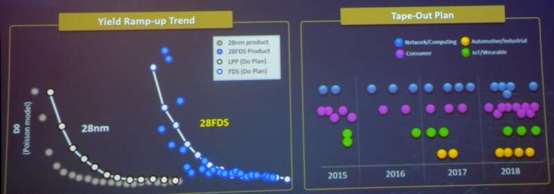
Samsung said its 28nm FDS now has mature yields and an expanding set of customers. Click to enlarge. Source: Samsung
NXP plans to use Samsung’s embedded MRAM now being readied for the 28nm node. It also will apply a handful of body biasing techniques on different chips.
“If you don’t invest in body basing, you won’t get leadership results,” said Ron Martino who runs NXP’s i.MX group.
Hong Hao, head of Samsung’s foundry group, said he has mature yields and a growing customer set for 28nm FDS. He showed a list of more than a dozen IP blocks verified in silicon including DDR2-4, USB 2-3, PCIe Gen 2-4, Gigabit Ethernet, SATA Gen3 and MIPI M- and D-PHY interfaces.
The South Korean giant provides design guides for body biasing and has automotive Grade-1 capability in place with Grade-2 coming by midyear.
Samsung plans to ramp late next year an 18nm FDS capable of 24 percent more performance, 38 percent less power consumption and 35 percent less area with early design kits due in September. Rival GF aims to ramp a 12nm FDX node in Dresden in the second half of 2020.
Andes preps RISC-V core for Linux
In December, Taiwan-based IP provider Andes announced a technology transition of its own — to the emerging RISC-V architecture. Chief executive Frankwell Lin used his keynote at the event to announce the company will release in July a version of its RISC-V-based N25 core for Linux.
Andes already has signed up a vendor of enterprise solid-state drives to use its existing N25 running an RTOS in a flash controller. A design services company also signed up to use the 32-bit core for which a 64-bit derivative is in the works.
Many engineers following RISC-V have had at the top of their wish lists for some time a chip that boots Linux. Startup SiFive just started sampling boards with its own version of such a chip that is part of its design library.
Andes hopes to differentiate its offering in part with its Copilot tool that helps users add custom instructions to their designs. It has signed up two design services companies ready to work with the Linux core.
To date Andes has had modest financial success, but it has had a significant impact on SoC designs. The company which reported 2017 revenues of just $9 million, said it sold licenses for 590 million of its proprietary cores last year and 2.5 billion to date.
On the process front, Lin praised FD-SOI for using 30 percent fewer masks than FinFET processes as well as for its low power and support of RF. He described a 2015 test chip Andes designed in GF’s 22n FDX that in simulations outperformed 28nm ULP nodes.
The IP provider is working with partners on its first deal for an FD-SOI design, but the customer has not yet signed.
Sony is one of the farthest along the FD-SOI road. It went into production at ST with a GPS chip in 2015 designed into several watches and now has a more integrated follow-on designed into the company’s Xperia ear buds.
The initial chip dropped power consumption to 1.5 mW from 6.3mW for a prior design, said Kenichi Nakano, general manager of Sony Semiconductor’s IoT division. The company plans a version with CatM and NB-IoT cellular later this year and is already working on designs for 2019, he said.
In a sign of how quickly things have turned around, the chief executive of SOI wafer vendor Soitec said his company was facing the prospect of bankruptcy three years ago. Now its ramping a new plant in Singapore and aims to ship as many as 600,000 300mm wafers this year and many more 200mm wafers for use in smartphone RF front ends and other designs.

Andes will release in July a derivative of its 32-bit N25 RISC-V core for Linux. Click to enlarge. Source: Andes
— Rick Merritt, Silicon Valley Bureau Chief, EE Times

Subscribe to Newsletter

Test Qr code text s ss
