2nm: End of the Road?
Article By : Rick Merritt

The law of diminishing returns may prove anything smaller than 5nm difficult
SANTA CLARA, Calif. — Engineers see many options to create 5-, 3- and even 2-nm semiconductor process technologies, but some are not sure that they will be able to squeeze commercial advantages from them even at 5 nm.
The increasing complexity and cost of making ever-smaller chips is leading to diminishing returns. Data rates are peaking at 3 GHz for mobile processors, and power and area gains will narrow at 7 nm, said a Qualcomm engineer in a panel at a Synopsys user group event here.
Speed gains of 16% at 10 nm may dry up at 7 nm due to resistance in metal lines. Power savings will shrink from 30% at 10 nm to 10–25% at 7 nm, and area shrinks may decline from 37% at 10 nm to 20–30% at 7 nm, said Paul Penzes, a senior director of engineering on Qualcomm’s design technology team.
For decades, the electronics industry followed a roadmap codified by Moore’s law of doubling the number of transistors on a chip roughly every two years. The result was a fast pace of ever-smaller, faster, cheaper products from PCs to smartphones.
“Area still scales in strong double digits, but the hidden cost increases in masks means the actual cost advantages and other improvements are starting to slow down … It’s not clear what will remain at 5 nm,” said Penzes, suggesting that 5-nm nodes may only be extensions of 7 nm.
Versions of today’s FinFET transistors will be used down to the 5-nm node, said technologists from Synopsys and Samsung on the panel. Below a width of about 3.5 nm, FinFETs will hit a hard limit.
Designers will need to transition to a stack of probably three thin horizontal nanowires sometimes called nano-slabs, said Victor Moroz, a fellow and transistor expert at Synopsys. For its part, Samsung has announced plans to use a gate-all-around transistor for a 4-nm process that it aims to have in production by 2020.
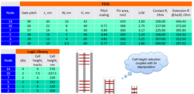
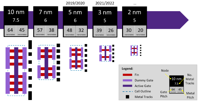
At future nodes, pitch scaling will slow to about 0.8x per generation, according to Munoz of Synopsys. That will force designers to shrink cell heights from about 228 nm with two fins and six tracks at 7 nm to 130–100 nm with five tracks and a single fin at 3 and 2 nm, he said.
Using such techniques, “silicon looks to safely take us to 2 nm, and after that, we may look to graphene,” he concluded.
However, in a Q&A session, one attendee expressed shock at the idea of a five-track cell with a single fin.
Synopsys sketched out a generic roadmap to 2 nm to start discussion on a panel. Source: Synopsys.
Confidence remains a key ingredient
The complexity of finer processes has tied chip designers to increasingly restrictive design rules, said Henry Sheng, a group R&D director at Synopsys. For instance, FinFETs brought new effects in waveform propagation, electro-migration, and device variations that engineers need to track.
“The abstractions we worked so hard to maintain are becoming porous as secondary and tertiary effects bubble up through the whole flow … from node to node, they intensify or change character,” he said, expressing optimism that “all of these effects will get solved.”
Panelists agreed that success depends on increasingly tight collaboration among foundry, EDA, and design engineers. Toward that goal, Qualcomm found that, to get optimal yields, it needs to tweak its leading-edge designs just before production starts, when the process node is more clearly defined.
“Because mobile processors are so competitive, foundries are putting in front of us less and less mature nodes,” said Penzes. “If you over-margin, then average unit cost goes up, and we are not competitive.”
“Today, you have to know quite a bit about the environment of a cell before you know its electrical characteristics,” he added. “Variations of 10% could take away the full advantage of a new process, so things that used to be noise can’t be left on the table.”
Penzes noted some recent work raising hopes. Foundries are finding ways to scale different cells at different rates, and EDA vendors promise improved routing, perhaps with help from extreme ultraviolet lithography (EUV).
Moroz of Synopsys said that engineers are also exploring many techniques to reduce resistance on metal lines that could open a door to speed gains. They include new structures such as via ladders and super-vias that span multiple metal layers as well as use of new materials such as cobalt and ruthenium.

Moroz fleshed out a roadmap in more detail to illustrate challenges ahead. Source: Synopsys.
A perennial ingredient for success continues to be raw confidence that engineers will find ways to solve thorny problems.
For example, Samsung has committed to specs for a 7-nm process with EUV and plans to make wafers this year, although it is still waiting on steppers. “As soon as ASML can deliver the tools, we are committed to high-volume manufacturing,” said Jongwook Kye, a vice president of design enablement for Samsung Foundry, on the panel.
Meanwhile, the South Korean chip giant is trying to define a new transistor for 4-nm production in 2020. “That’s a challenge we need to solve over the next couple of years, and as long as we collaborate with tool vendors and others, I believe we can achieve it,” said Kye.
— Rick Merritt, Silicon Valley Bureau Chief, EE Times 
Subscribe to Newsletter
Test Qr code text s ss


